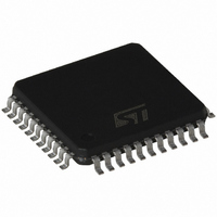
ST72F324LJ2T5 STMicroelectronics, ST72F324LJ2T5 Datasheet - Page 132

ST72F324LJ2T5
Manufacturer Part Number
ST72F324LJ2T5
Description
IC MCU 8BIT 8K FLASH 44-LQFP
Manufacturer
STMicroelectronics
Series
ST7r
Datasheet
1.ST72F324LJ2T5.pdf
(154 pages)
Specifications of ST72F324LJ2T5
Core Processor
ST7
Core Size
8-Bit
Speed
8MHz
Connectivity
SCI, SPI
Peripherals
POR, PWM, WDT
Number Of I /o
32
Program Memory Size
8KB (8K x 8)
Program Memory Type
FLASH
Ram Size
384 x 8
Voltage - Supply (vcc/vdd)
2.85 V ~ 3.6 V
Data Converters
A/D 12x10b
Oscillator Type
Internal
Operating Temperature
-10°C ~ 85°C
Package / Case
44-LQFP
Processor Series
ST72F3x
Core
ST7
Data Bus Width
8 bit
Data Ram Size
384 B
Interface Type
SCI, SPI
Maximum Clock Frequency
8 MHz
Number Of Programmable I/os
32
Number Of Timers
2
Maximum Operating Temperature
+ 85 C
Mounting Style
SMD/SMT
Development Tools By Supplier
ST7232X-EVAL, ST7MDT20-DVP3, ST7MDT20J-EMU3, STX-RLINK
Minimum Operating Temperature
- 10 C
On-chip Adc
10 bit, 12 Channel
For Use With
497-6421 - BOARD EVAL DGTL BATT CHGR DESIGN497-5046 - KIT TOOL FOR ST7/UPSD/STR7 MCU
Lead Free Status / RoHS Status
Lead free / RoHS Compliant
Eeprom Size
-
Lead Free Status / Rohs Status
Details
Other names
497-8242
ST72F324LJ2T5
ST72F324LJ2T5
Available stocks
Company
Part Number
Manufacturer
Quantity
Price
Company:
Part Number:
ST72F324LJ2T5
Manufacturer:
STMicroelectronics
Quantity:
10 000
Part Number:
ST72F324LJ2T5
Manufacturer:
ST
Quantity:
20 000
Company:
Part Number:
ST72F324LJ2T5TR
Manufacturer:
STMicroelectronics
Quantity:
10 000
ST72324Lxx
12.12 10-BIT ADC CHARACTERISTICS
Subject to general operating conditions for V
Figure 78. R
Notes:
1. When V
2. Any added external serial resistor will downgrade the ADC accuracy (especially for resistance greater than 10kΩ). Data
based on characterization results, not tested in production.
3. C
pacitance (3pF). A high C
4. This graph shows that depending on the input signal variation (f
decreased to allow the use of a larger serial resistor (R
5.The analog inputs of ROM devices are designed to be negative current tolerant. On Flash devices, injecting negative
current on any of the analog input pins significantly reduces the accuracy of any conversion being performed on any an-
alog input.
Analog pins can be protected against negative injection by adding a Schottky diode (pin to ground). Injecting negative
current on digital input pins degrades ADC accuracy especially if performed on a pin close to the analog input pins.
Any positive injection current within the limits specified for I
accuracy.
132/154
1
Symbol
V
C
R
C
f
V
t
t
f
AREF
ADC
ADC
ADC
I
PARASITIC
AIN
ADC
lkg
AIN
AIN
AIN
45
40
35
30
25
20
15
10
5
0
AREF
ADC clock frequency
Analog reference voltage
Conversion voltage range
Positive input leakage current for analog
input
ROM devices: negative input leakage
current on analog pins
External input impedance
External capacitor on analog input
Variation freq. of analog input signal
Internal sample and hold capacitor
Conversion time (Sample+Hold)
f
- No of sample capacitor loading cycles
- No. of Hold conversion cycles
CPU
0
represents the capacitance of the PCB (dependent on soldering and PCB layout quality) plus the pad ca-
AIN
and V
=4MHz, SPEED=0 f
max. vs f
SSA
10
C
PARASITIC
PARASITIC
Parameter
pins are not available on the pinout, the ADC refers to V
ADC
(pF)
30
5)
with C
value will downgrade conversion accuracy. To remedy this, f
ADC
1)
2)
=1MHz
1 MHz
AIN
70
=0pF
DD
3)
-40°C≤T
V
on adjacent analog pin
, f
IN
AIN)
CPU
<
V
.
INJ(PIN)
Conditions
SS,
, and T
A
Figure 79. Recommended C
≤85°C range
| I
IN
1000
and ΣI
AIN
100
|< 400µA
0.1
10
1
A
), C
unless otherwise specified.
INJ(PIN)
AIN
0.01
can be increased for stabilization time and
V
in
Min
V
0.4
SSA
DD
DD
Section 12.8
0.1
and V
f
AIN
(KHz)
Typ
SS
12
5
15
11
4
.
1
does not affect the ADC
ADC
AIN
Cain 10 nF
Cain 22 nF
Cain 47 nF
Figure 78
79
should be reduced.
& R
Figure
V
Max
see
and
V
AREF
2)3)4)
1
1
6
DD
10
AIN values.
1/f
Unit
MHz
µA
µA
kΩ
pF
Hz
pF
µs
V
ADC
4)


