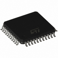
ST72F324LJ2T5 STMicroelectronics, ST72F324LJ2T5 Datasheet - Page 25

ST72F324LJ2T5
Manufacturer Part Number
ST72F324LJ2T5
Description
IC MCU 8BIT 8K FLASH 44-LQFP
Manufacturer
STMicroelectronics
Series
ST7r
Datasheet
1.ST72F324LJ2T5.pdf
(154 pages)
Specifications of ST72F324LJ2T5
Core Processor
ST7
Core Size
8-Bit
Speed
8MHz
Connectivity
SCI, SPI
Peripherals
POR, PWM, WDT
Number Of I /o
32
Program Memory Size
8KB (8K x 8)
Program Memory Type
FLASH
Ram Size
384 x 8
Voltage - Supply (vcc/vdd)
2.85 V ~ 3.6 V
Data Converters
A/D 12x10b
Oscillator Type
Internal
Operating Temperature
-10°C ~ 85°C
Package / Case
44-LQFP
Processor Series
ST72F3x
Core
ST7
Data Bus Width
8 bit
Data Ram Size
384 B
Interface Type
SCI, SPI
Maximum Clock Frequency
8 MHz
Number Of Programmable I/os
32
Number Of Timers
2
Maximum Operating Temperature
+ 85 C
Mounting Style
SMD/SMT
Development Tools By Supplier
ST7232X-EVAL, ST7MDT20-DVP3, ST7MDT20J-EMU3, STX-RLINK
Minimum Operating Temperature
- 10 C
On-chip Adc
10 bit, 12 Channel
For Use With
497-6421 - BOARD EVAL DGTL BATT CHGR DESIGN497-5046 - KIT TOOL FOR ST7/UPSD/STR7 MCU
Lead Free Status / RoHS Status
Lead free / RoHS Compliant
Eeprom Size
-
Lead Free Status / Rohs Status
Details
Other names
497-8242
ST72F324LJ2T5
ST72F324LJ2T5
Available stocks
Company
Part Number
Manufacturer
Quantity
Price
Company:
Part Number:
ST72F324LJ2T5
Manufacturer:
STMicroelectronics
Quantity:
10 000
Part Number:
ST72F324LJ2T5
Manufacturer:
ST
Quantity:
20 000
Company:
Part Number:
ST72F324LJ2T5TR
Manufacturer:
STMicroelectronics
Quantity:
10 000
6.3 RESET SEQUENCE MANAGER (RSM)
6.3.1 Introduction
The reset sequence manager includes two RE-
SET sources as shown in
■
■
These sources act on the RESET pin and it is al-
ways kept low during the delay phase.
The RESET service routine vector is fixed at ad-
dresses FFFEh-FFFFh in the ST7 memory map.
The basic RESET sequence consists of 3 phases
as shown in
■
■
■
The 256 or 4096 CPU clock cycle delay allows the
oscillator to stabilise and ensures that recovery
has taken place from the Reset state. The shorter
or longer clock cycle delay should be selected by
option byte to correspond to the stabilization time
of the external oscillator used in the application.
The RESET vector fetch phase duration is 2 clock
cycles.
Figure 12. RESET Sequence Phases
Figure 13. Reset Block Diagram
External RESET source pulse
Internal WATCHDOG RESET
Active Phase depending on the RESET source
256 or 4096 CPU clock cycle delay (selected by
option byte)
RESET vector fetch
RESET
Active Phase
Figure
256 or 4096 CLOCK CYCLES
12:
INTERNAL RESET
RESET
V
Figure
DD
R
ON
13:
VECTOR
FETCH
Filter
6.3.2 Asynchronous External RESET pin
The RESET pin is both an input and an open-drain
output with integrated R
This pull-up has no fixed value but varies in ac-
cordance with the input voltage. It can be pulled
low by external circuitry to reset the device. See
Electrical Characteristic section for more details.
A RESET signal originating from an external
source must have a duration of at least t
order to be recognized. This detection is asynchro-
nous and therefore the MCU can enter reset state
even in HALT mode.
The RESET pin is an asynchronous signal which
plays a major role in EMS performance. In a noisy
environment, it is recommended to follow the
guidelines mentioned in the electrical characteris-
tics section.
6.3.3 External Power-On RESET
To start up the microcontroller correctly, the user
must ensure by means of an external reset circuit
that the reset signal is held low until V
the minimum level specified for the selected f
frequency.
A proper reset signal for a slow rising V
can generally be provided by an external RC net-
work connected to the RESET pin.
6.3.4 Internal Watchdog RESET
Starting from the Watchdog counter underflow, the
device RESET pin acts as an output that is pulled
low during at least t
GENERATOR
PULSE
WATCHDOG RESET
w(RSTL)out
ON
weak pull-up resistor.
.
INTERNAL
RESET
ST72324Lxx
h(RSTL)in
DD
DD
is over
supply
25/154
OSC
in
1


