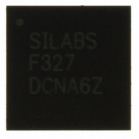
C8051F327-GM Silicon Laboratories Inc, C8051F327-GM Datasheet - Page 101

C8051F327-GM
Manufacturer Part Number
C8051F327-GM
Description
IC 8051 MCU FLASH 16K 28QFN
Manufacturer
Silicon Laboratories Inc
Series
C8051F32xr
Specifications of C8051F327-GM
Program Memory Type
FLASH
Program Memory Size
16KB (16K x 8)
Package / Case
28-QFN
Core Processor
8051
Core Size
8-Bit
Speed
25MHz
Connectivity
UART/USART, USB
Peripherals
POR
Number Of I /o
15
Ram Size
1.5K x 8
Voltage - Supply (vcc/vdd)
2.7 V ~ 3.6 V
Oscillator Type
Internal
Operating Temperature
-40°C ~ 85°C
Processor Series
C8051F3x
Core
8051
Data Bus Width
8 bit
Data Ram Size
1.5 KB
Interface Type
UART/USB
Maximum Clock Frequency
25 MHz
Number Of Programmable I/os
15
Number Of Timers
2
Operating Supply Voltage
2.7 V to 3.6 V
Maximum Operating Temperature
+ 85 C
Mounting Style
SMD/SMT
3rd Party Development Tools
PK51, CA51, A51, ULINK2
Development Tools By Supplier
C8051F326DK
Minimum Operating Temperature
- 40 C
Package
28QFN EP
Device Core
8051
Family Name
C8051F327
Maximum Speed
25 MHz
Lead Free Status / RoHS Status
Lead free / RoHS Compliant
For Use With
336-1481 - DAUGHTER CARD TOOLSTCK C8051F327770-1006 - ISP 4PORT FOR SILABS C8051F MCU
Eeprom Size
-
Data Converters
-
Lead Free Status / Rohs Status
Lead free / RoHS Compliant
Other names
336-1297-5
Available stocks
Company
Part Number
Manufacturer
Quantity
Price
Part Number:
C8051F327-GM
Manufacturer:
SILICON LABS/芯科
Quantity:
20 000
12.8. Interrupts
The read-only USB0 interrupt flags are located in the USB registers shown in Figure 12.11 through
Figure 12.13. The associated interrupt enable bits are located in the USB registers shown in Figure 12.14
through Figure 12.16. A USB0 interrupt is generated when any of the USB interrupt flags is set to ‘1’. The
USB0 interrupt is enabled via the EIE1 SFR (see Section “6.3. Interrupt Handler” on page 48).
Important Note: Reading a USB interrupt flag register resets all flags in that register to ‘0’.
Bits7–2: Unused. Read = 000000b. Write = don’t care.
Bit1:
Bit0:
Bits7–2: Unused. Read = 000000b. Write = don’t care.
Bit1:
Bit0:
Bit7
Bit7
—
—
R
R
USB Register Definition 12.12. OUT1INT: USB0 Out Endpoint Interrupt
USB Register Definition 12.11. IN1INT: USB0 IN Endpoint Interrupt
IN1: IN Endpoint 1 Interrupt-pending Flag
This bit is cleared when software reads the IN1INT register.
0: IN Endpoint 1 interrupt inactive.
1: IN Endpoint 1 interrupt active.
EP0: Endpoint 0 Interrupt-pending Flag
This bit is cleared when software reads the IN1INT register.
0: Endpoint 0 interrupt inactive.
1: Endpoint 0 interrupt active.
OUT1: OUT Endpoint 1 Interrupt-pending Flag
This bit is cleared when software reads the OUT1INT register.
0: OUT Endpoint 1 interrupt inactive.
1: OUT Endpoint 1 interrupt active.
Unused. Read = 0. Write = don’t care.
Bit6
Bit6
—
—
R
R
Bit5
Bit5
—
—
R
R
Bit4
Bit4
—
—
R
R
Rev. 1.1
Bit3
Bit3
—
—
R
R
Bit2
Bit2
—
—
R
R
OUT1
IN1
Bit1
Bit1
R
R
C8051F326/7
EP0
Bit0
Bit0
—
R
R
USB Address:
USB Address:
00000000
00000000
Reset Value
Reset Value
0x04
0x02
101


