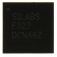
C8051F327-GM Silicon Laboratories Inc, C8051F327-GM Datasheet - Page 120

C8051F327-GM
Manufacturer Part Number
C8051F327-GM
Description
IC 8051 MCU FLASH 16K 28QFN
Manufacturer
Silicon Laboratories Inc
Series
C8051F32xr
Specifications of C8051F327-GM
Program Memory Type
FLASH
Program Memory Size
16KB (16K x 8)
Package / Case
28-QFN
Core Processor
8051
Core Size
8-Bit
Speed
25MHz
Connectivity
UART/USART, USB
Peripherals
POR
Number Of I /o
15
Ram Size
1.5K x 8
Voltage - Supply (vcc/vdd)
2.7 V ~ 3.6 V
Oscillator Type
Internal
Operating Temperature
-40°C ~ 85°C
Processor Series
C8051F3x
Core
8051
Data Bus Width
8 bit
Data Ram Size
1.5 KB
Interface Type
UART/USB
Maximum Clock Frequency
25 MHz
Number Of Programmable I/os
15
Number Of Timers
2
Operating Supply Voltage
2.7 V to 3.6 V
Maximum Operating Temperature
+ 85 C
Mounting Style
SMD/SMT
3rd Party Development Tools
PK51, CA51, A51, ULINK2
Development Tools By Supplier
C8051F326DK
Minimum Operating Temperature
- 40 C
Package
28QFN EP
Device Core
8051
Family Name
C8051F327
Maximum Speed
25 MHz
Lead Free Status / RoHS Status
Lead free / RoHS Compliant
For Use With
336-1481 - DAUGHTER CARD TOOLSTCK C8051F327770-1006 - ISP 4PORT FOR SILABS C8051F MCU
Eeprom Size
-
Data Converters
-
Lead Free Status / Rohs Status
Lead free / RoHS Compliant
Other names
336-1297-5
Available stocks
Company
Part Number
Manufacturer
Quantity
Price
Part Number:
C8051F327-GM
Manufacturer:
SILICON LABS/芯科
Quantity:
20 000
C8051F326/7
13.2. Data Format
UART0 has a number of available options for data formatting. Data transfers begin with a start bit (logic
low), followed by the data bits (sent LSB-first), a parity or extra bit (if selected), and end with one or two
stop bits (logic high). The data length is variable between 5 and 8 bits. A parity bit can be appended to the
data, and automatically generated and detected by hardware for even, odd, mark, or space parity. The stop
bit length is selectable between 1 and 2 bit times, and a multi-processor communication mode is available
for implementing networked UART buses. All of the data formatting options can be configured using the
SMOD0 register, shown in SFR Definition 13.2. Figure 13.2 shows the timing for a UART0 transaction
without parity or an extra bit enabled. Figure 13.3 shows the timing for a UART0 transaction with parity
enabled (PE0 = 1). Figure 13.4 is an example of a UART0 transaction when the extra bit is enabled
(XBE0 = 1). Note that the extra bit feature is not available when parity is enabled, and the second stop bit
is only an option for data lengths of 6, 7, or 8 bits.
120
SPACE
SPACE
MARK
MARK
BIT TIMES
BIT TIMES
SPACE
MARK
BIT TIMES
START
START
BIT
BIT
Figure 13.2. UART0 Timing Without Parity or Extra Bit
START
BIT
D
D
Figure 13.4. UART0 Timing With Extra Bit
0
0
Figure 13.3. UART0 Timing With Parity
D
0
D
D
1
1
N bits; N = 5, 6, 7, or 8
N bits; N = 5, 6, 7, or 8
D
1
N bits; N = 5, 6, 7, or 8
Rev. 1.1
D
D
N-2
N-2
D
N-2
D
D
N-1
N-1
D
N-1
PARITY
EXTRA
STOP
BIT 1
STOP
STOP
BIT 1
BIT 1
Optional
(6,7,8 bit
STOP
BIT 2
Data)
Optional
Optional
(6,7,8 bit
(6,7,8 bit
STOP
STOP
BIT 2
Data)
BIT 2
Data)


