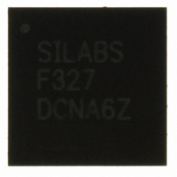
C8051F327-GM Silicon Laboratories Inc, C8051F327-GM Datasheet - Page 138

C8051F327-GM
Manufacturer Part Number
C8051F327-GM
Description
IC 8051 MCU FLASH 16K 28QFN
Manufacturer
Silicon Laboratories Inc
Series
C8051F32xr
Specifications of C8051F327-GM
Program Memory Type
FLASH
Program Memory Size
16KB (16K x 8)
Package / Case
28-QFN
Core Processor
8051
Core Size
8-Bit
Speed
25MHz
Connectivity
UART/USART, USB
Peripherals
POR
Number Of I /o
15
Ram Size
1.5K x 8
Voltage - Supply (vcc/vdd)
2.7 V ~ 3.6 V
Oscillator Type
Internal
Operating Temperature
-40°C ~ 85°C
Processor Series
C8051F3x
Core
8051
Data Bus Width
8 bit
Data Ram Size
1.5 KB
Interface Type
UART/USB
Maximum Clock Frequency
25 MHz
Number Of Programmable I/os
15
Number Of Timers
2
Operating Supply Voltage
2.7 V to 3.6 V
Maximum Operating Temperature
+ 85 C
Mounting Style
SMD/SMT
3rd Party Development Tools
PK51, CA51, A51, ULINK2
Development Tools By Supplier
C8051F326DK
Minimum Operating Temperature
- 40 C
Package
28QFN EP
Device Core
8051
Family Name
C8051F327
Maximum Speed
25 MHz
Lead Free Status / RoHS Status
Lead free / RoHS Compliant
For Use With
336-1481 - DAUGHTER CARD TOOLSTCK C8051F327770-1006 - ISP 4PORT FOR SILABS C8051F MCU
Eeprom Size
-
Data Converters
-
Lead Free Status / Rohs Status
Lead free / RoHS Compliant
Other names
336-1297-5
Available stocks
Company
Part Number
Manufacturer
Quantity
Price
Part Number:
C8051F327-GM
Manufacturer:
SILICON LABS/芯科
Quantity:
20 000
C8051F326/7
D
Revision 0.5 to Revision 1.0
•
•
•
•
•
•
•
•
•
•
•
Revision 1.0 to Revision 1.1
•
138
OCUMENT
Updated Section “1. System Overview” on page 13 and Table 1.1, “Product Selection Guide,” on
page 13.
-
Added Figure 1.3. "Typical Connections for the C8051F326" on page 16 and Figure 1.4. "Typical Con-
nections for the C8051F327" on page 16.
Changed Figure 4.5. "Typical C8051F327 QFN-28 Landing Diagram" on page 31 to show ground con-
nection on Pin 3.
Replaced TBDs with values in Table 5.1, “Voltage Regulator Electrical Specifications,” on page 31.
Replaced TBDs with values in Table 7.1, “Reset Electrical Characteristics,” on page 62.
Moved USB Active characteristics from Table 3.1, “Global DC Electrical Characteristics,” on page 24 to
Table 12.4, “USB Transceiver Electrical Characteristics,” on page 115.
Added port information to Figure 11.1. "Port I/O Functional Block Diagram" on page 79.
Added read/write state description to bits 7–6 in SFR Definition 11.4. “P2: Port2” on page 83.
Clarified description of read state for bits 7–3 in USB Register Definition 12.10. “FRAMEH: USB0
Frame Number High” on page 100.
Clarified description of read state for bits 7–2 in USB Register Definition 12.24. “EOUTCNTH: USB0
OUT Endpoint Count High” on page 114.
Standardized descriptions for “unused” and “reserved” bits in SFR Definitions throughout document.
Updated package and land pattern drawings.
Changed “-GQ” references to “-GM”
C
HANGE
L
IST
Rev. 1.1


