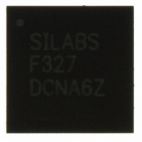
C8051F327-GM Silicon Laboratories Inc, C8051F327-GM Datasheet - Page 75

C8051F327-GM
Manufacturer Part Number
C8051F327-GM
Description
IC 8051 MCU FLASH 16K 28QFN
Manufacturer
Silicon Laboratories Inc
Series
C8051F32xr
Specifications of C8051F327-GM
Program Memory Type
FLASH
Program Memory Size
16KB (16K x 8)
Package / Case
28-QFN
Core Processor
8051
Core Size
8-Bit
Speed
25MHz
Connectivity
UART/USART, USB
Peripherals
POR
Number Of I /o
15
Ram Size
1.5K x 8
Voltage - Supply (vcc/vdd)
2.7 V ~ 3.6 V
Oscillator Type
Internal
Operating Temperature
-40°C ~ 85°C
Processor Series
C8051F3x
Core
8051
Data Bus Width
8 bit
Data Ram Size
1.5 KB
Interface Type
UART/USB
Maximum Clock Frequency
25 MHz
Number Of Programmable I/os
15
Number Of Timers
2
Operating Supply Voltage
2.7 V to 3.6 V
Maximum Operating Temperature
+ 85 C
Mounting Style
SMD/SMT
3rd Party Development Tools
PK51, CA51, A51, ULINK2
Development Tools By Supplier
C8051F326DK
Minimum Operating Temperature
- 40 C
Package
28QFN EP
Device Core
8051
Family Name
C8051F327
Maximum Speed
25 MHz
Lead Free Status / RoHS Status
Lead free / RoHS Compliant
For Use With
336-1481 - DAUGHTER CARD TOOLSTCK C8051F327770-1006 - ISP 4PORT FOR SILABS C8051F MCU
Eeprom Size
-
Data Converters
-
Lead Free Status / Rohs Status
Lead free / RoHS Compliant
Other names
336-1297-5
Available stocks
Company
Part Number
Manufacturer
Quantity
Price
Part Number:
C8051F327-GM
Manufacturer:
SILICON LABS/芯科
Quantity:
20 000
10.4. 4x Clock Multiplier
The 4x Clock Multiplier allows a 12 MHz oscillator to generate the 48 MHz clock required for Full Speed
USB communication (see Section “12.4. USB Clock Configuration” on page 94). A divided version of the
Multiplier output can also be used as the system clock. See Section “10.5. System and USB Clock Selec-
tion” on page 76 for details on system clock and USB clock source selection.
The 4x Clock Multiplier is configured via the CLKMUL register. The procedure for configuring and enabling
the 4x Clock Multiplier is as follows:
Important Note: When using an external clock as the input to the 4x Clock Multiplier, the external source
must be stable before the Multiplier is initialized. See Section “10.5. System and USB Clock Selection” on
page 76 for details on clock selection.
Bit7:
Bit6:
Bit5:
Bits4–1: Unused. Read = 0000b. Write = don’t care.
Bit0:
MULEN
R/W
Bit7
1. Reset the Multiplier by writing 0x00 to register CLKMUL.
2. Select the Multiplier input source via the MULSEL bits.
3. Enable the Multiplier with the MULEN bit (CLKMUL | = 0x80).
4. Delay for >5 µs.
5. Initialize the Multiplier with the MULINIT bit (CLKMUL | = 0xC0).
6. Poll for MULRDY => ‘1’.
MULEN: Clock Multiplier Enable
0: Clock Multiplier disabled.
1: Clock Multiplier enabled.
MULINIT: Clock Multiplier Initialize
This bit should be a ‘0’ when the Clock Multiplier is enabled. Once enabled, writing a ‘1’ to
this bit will initialize the Clock Multiplier. The MULRDY bit reads ‘1’ when the Clock Multiplier
is stabilized.
MULRDY: Clock Multiplier Ready
This read-only bit indicates the status of the Clock Multiplier.
0: Clock Multiplier not ready.
1: Clock Multiplier ready (locked).
MULSEL: Clock Multiplier Input Select
This bit selects the clock supplied to the Clock Multiplier.
MULINIT MULRDY
R/W
Bit6
SFR Definition 10.4. CLKMUL: Clock Multiplier Control
MULSEL
0
1
Bit5
R
R/W
Bit4
—
Internal Oscillator
Selected Clock
External Clock
Rev. 1.1
R/W
Bit3
—
R/W
Bit2
—
R/W
Bit1
—
C8051F326/7
MULSEL 00000000
R/W
Bit0
SFR Address
Reset Value
0xB9
75


