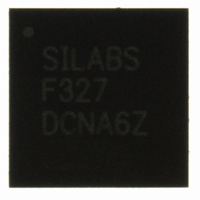
C8051F327-GM Silicon Laboratories Inc, C8051F327-GM Datasheet - Page 132

C8051F327-GM
Manufacturer Part Number
C8051F327-GM
Description
IC 8051 MCU FLASH 16K 28QFN
Manufacturer
Silicon Laboratories Inc
Series
C8051F32xr
Specifications of C8051F327-GM
Program Memory Type
FLASH
Program Memory Size
16KB (16K x 8)
Package / Case
28-QFN
Core Processor
8051
Core Size
8-Bit
Speed
25MHz
Connectivity
UART/USART, USB
Peripherals
POR
Number Of I /o
15
Ram Size
1.5K x 8
Voltage - Supply (vcc/vdd)
2.7 V ~ 3.6 V
Oscillator Type
Internal
Operating Temperature
-40°C ~ 85°C
Processor Series
C8051F3x
Core
8051
Data Bus Width
8 bit
Data Ram Size
1.5 KB
Interface Type
UART/USB
Maximum Clock Frequency
25 MHz
Number Of Programmable I/os
15
Number Of Timers
2
Operating Supply Voltage
2.7 V to 3.6 V
Maximum Operating Temperature
+ 85 C
Mounting Style
SMD/SMT
3rd Party Development Tools
PK51, CA51, A51, ULINK2
Development Tools By Supplier
C8051F326DK
Minimum Operating Temperature
- 40 C
Package
28QFN EP
Device Core
8051
Family Name
C8051F327
Maximum Speed
25 MHz
Lead Free Status / RoHS Status
Lead free / RoHS Compliant
For Use With
336-1481 - DAUGHTER CARD TOOLSTCK C8051F327770-1006 - ISP 4PORT FOR SILABS C8051F MCU
Eeprom Size
-
Data Converters
-
Lead Free Status / Rohs Status
Lead free / RoHS Compliant
Other names
336-1297-5
Available stocks
Company
Part Number
Manufacturer
Quantity
Price
Part Number:
C8051F327-GM
Manufacturer:
SILICON LABS/芯科
Quantity:
20 000
C8051F326/7
132
Bit7:
Bit6:
Bits5–4: T1M1-T1M0: Timer 1 Mode Select.
Bit3:
Bit2:
Bits1–0: T0M1-T0M0: Timer 0 Mode Select.
GATE1
R/W
Bit7
GATE1: Timer 1 Gate Control.
0: Timer 1 enabled when TR1 = 1 irrespective of /INT1 logic level. /INT1 is activated when
the internal oscillator resumes from a suspended state.
1: Timer 1 enabled only when TR1 = 1 AND /INT1 is active. /INT1 is activated every 2 low
frequency oscillator clock cycles. This is a rate of 40kHz.
Reserved. Read = 0b. Must write 0b.
These bits select the Timer 1 operation mode.
GATE0: Timer 0 Gate Control.
0: Timer 0 enabled when TR0 = 1 irrespective of /INT0 logic level. /INT0 input pin is P0.0.
1: Timer 0 enabled only when TR0 = 1 AND /INT0 is active. /INT0 input pin is P0.2.
Reserved. Read = 0b. Must write 0b.
These bits select the Timer 0 operation mode.
Reserved
T1M1
T0M1
0
0
1
1
0
0
1
1
R/W
Bit6
T1M0
T0M0
0
1
0
1
0
1
0
1
SFR Definition 14.2. TMOD: Timer Mode
T1M1
R/W
Bit5
Mode 2: 8-bit timer with auto-reload
Mode 2: 8-bit timer with auto-reload
T1M0
R/W
Bit4
Mode 3: Timer 1 inactive
Mode 3: Two 8-bit timers
Mode 0: 13-bit timer
Mode 1: 16-bit timer
Mode 0: 13-bit timer
Mode 1: 16-bit timer
Rev. 1.1
GATE0
Mode
Mode
R/W
Bit3
Reserved
R/W
Bit2
T0M1
R/W
Bit1
T0M0
R/W
Bit0
SFR Address:
00000000
Reset Value
0x89


