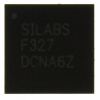
C8051F327-GM Silicon Laboratories Inc, C8051F327-GM Datasheet - Page 82

C8051F327-GM
Manufacturer Part Number
C8051F327-GM
Description
IC 8051 MCU FLASH 16K 28QFN
Manufacturer
Silicon Laboratories Inc
Series
C8051F32xr
Specifications of C8051F327-GM
Program Memory Type
FLASH
Program Memory Size
16KB (16K x 8)
Package / Case
28-QFN
Core Processor
8051
Core Size
8-Bit
Speed
25MHz
Connectivity
UART/USART, USB
Peripherals
POR
Number Of I /o
15
Ram Size
1.5K x 8
Voltage - Supply (vcc/vdd)
2.7 V ~ 3.6 V
Oscillator Type
Internal
Operating Temperature
-40°C ~ 85°C
Processor Series
C8051F3x
Core
8051
Data Bus Width
8 bit
Data Ram Size
1.5 KB
Interface Type
UART/USB
Maximum Clock Frequency
25 MHz
Number Of Programmable I/os
15
Number Of Timers
2
Operating Supply Voltage
2.7 V to 3.6 V
Maximum Operating Temperature
+ 85 C
Mounting Style
SMD/SMT
3rd Party Development Tools
PK51, CA51, A51, ULINK2
Development Tools By Supplier
C8051F326DK
Minimum Operating Temperature
- 40 C
Package
28QFN EP
Device Core
8051
Family Name
C8051F327
Maximum Speed
25 MHz
Lead Free Status / RoHS Status
Lead free / RoHS Compliant
For Use With
336-1481 - DAUGHTER CARD TOOLSTCK C8051F327770-1006 - ISP 4PORT FOR SILABS C8051F MCU
Eeprom Size
-
Data Converters
-
Lead Free Status / Rohs Status
Lead free / RoHS Compliant
Other names
336-1297-5
Available stocks
Company
Part Number
Manufacturer
Quantity
Price
Part Number:
C8051F327-GM
Manufacturer:
SILICON LABS/芯科
Quantity:
20 000
C8051F326/7
82
Bit7:
Bit6:
Bits5–1: Unused. Read = 00000b. Write = don’t care.
Bit0:
Bits7–0: P0.[7:0]
Bits7–0: Output Configuration Bits for P0.7-P0.0 (respectively):
WEAKPUD INPUTEN
P0.7
R/W
Bit7
R/W
Bit7
R/W
Bit7
WEAKPUD: Port I/O Weak Pullup Disable.
0: Weak Pullups enabled (except for I/O pins with Port latches set to logic 0 or are config-
ured to push-pull mode).
1: Weak Pullups disabled.
INPUTEN: Global Digital Input Enable.
0: Port I/O input path disabled; Port pins can be used as outputs only.
1: Port I/O input path enabled.
SYSCLK: /SYSCLK Enable
0: /SYSCLK unavailable at P0.0 pin. P0.0 Latch routed to P0.0 pin.
1: /SYSCLK routed to P0.0. P0.0 Latch unavailable at P0.0 pin.
Write - Output appears on I/O pins.
0: Logic Low Output.
1: Logic High Output (high impedance if corresponding P0MDOUT.n bit = 0).
Read - Always reads ‘0’ if INPUTEN = ‘0’. Otherwise, directly reads Port pin.
0: P0.n pin is logic low.
1: P0.n pin is logic high.
0: Corresponding P0.n Output is open-drain.
1: Corresponding P0.n Output is push-pull.
P0.6
R/W
Bit6
R/W
Bit6
R/W
Bit6
SFR Definition 11.1. GPIOCN: Global Port I/O Control
SFR Definition 11.3. P0MDOUT: Port0 Output Mode
P0.5
R/W
R/W
Bit5
Bit5
Bit5
—
R
SFR Definition 11.2. P0: Port0
P0.4
R/W
Bit4
R/W
Bit4
Bit4
—
R
Rev. 1.1
P0.3
R/W
Bit3
Bit3
R/W
Bit3
—
R
P0.2
Bit2
—
R/W
Bit2
R/W
Bit2
R
Bit1
P0.1
—
R
R/W
Bit1
R/W
Bit1
(bit addressable)
SYSCLK
R/W
Bit0
P0.0
R/W
Bit0
R/W
Bit0
SFR Address:
01000000
Reset Value
SFR Address:
SFR Address:
00000000
Reset Value
Reset Value
11111111
0xE2
0xA4
0x80


