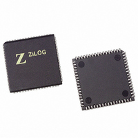
Z16F2810VH20EG Zilog, Z16F2810VH20EG Datasheet - Page 131

Z16F2810VH20EG
Manufacturer Part Number
Z16F2810VH20EG
Description
IC ZNEO MCU FLASH 128K 68PLCC
Manufacturer
Zilog
Series
Encore!® ZNEOr
Datasheet
1.Z16F2800100ZCOG.pdf
(388 pages)
Specifications of Z16F2810VH20EG
Core Processor
ZNEO
Core Size
16-Bit
Speed
20MHz
Connectivity
I²C, IrDA, LIN, SPI, UART/USART
Peripherals
Brown-out Detect/Reset, DMA, POR, PWM, WDT
Number Of I /o
46
Program Memory Size
128KB (128K x 8)
Program Memory Type
FLASH
Ram Size
4K x 8
Voltage - Supply (vcc/vdd)
2.7 V ~ 3.6 V
Data Converters
A/D 12x10b
Oscillator Type
Internal
Operating Temperature
-40°C ~ 105°C
Package / Case
68-LCC (J-Lead)
Data Bus Width
16 bit
Data Ram Size
4 B
Interface Type
ESPI, I2C, UART
Maximum Clock Frequency
20 MHz
Number Of Programmable I/os
46
Number Of Timers
4
Operating Supply Voltage
2.7 V to 3.6 V
Maximum Operating Temperature
+ 105 C
Mounting Style
SMD/SMT
Minimum Operating Temperature
- 40 C
On-chip Adc
10 bit, 12 Channel
For Use With
770-1003 - ISP 4PORT FOR ZILOG ZNEO MCU269-4537 - DEV KIT FOR Z16F ZNEO
Lead Free Status / RoHS Status
Lead free / RoHS Compliant
Eeprom Size
-
Lead Free Status / Rohs Status
Details
Other names
269-4691-5
Z16F2810VH20EG
Z16F2810VH20EG
Available stocks
Company
Part Number
Manufacturer
Quantity
Price
Company:
Part Number:
Z16F2810VH20EG
Manufacturer:
Zilog
Quantity:
151
- Current page: 131 of 388
- Download datasheet (22Mb)
PS022008-0810
PWM Reload Event
PWM Prescaler
PWM Period and Count Resolution
PWM Output Polarity and Off-State
The default off-state and polarity of the PWM outputs are controlled by the option bits
PWMHI and PWMLO. The PWMHI option controls the off-state and polarity for PWM
high-side outputs PWMH0, PWMH1, and PWMH2. The PWMLO option controls the
off-state and polarity for low-side outputs PWML0, PWML1, and PWML2.
The off-state is the value programmed in the option bit. For example, programming
to 1 makes the off-state of PWMH0, PWMH1, and PWMH2 a High logic value and the
active state a Low logic value. Conversely, programming PWMHI to 0 causes the off-state
to be a Low logic value. PWMLO is programmed in a similar manner.
PWM Enable
The MCEN option bit enables output pairs PWM0, PWM1, and PWM2. If the Motor
Control option is not enabled, the PWM outputs remain in a high-impedance state after
reset and is used as alternate functions like general purpose input. If the Motor Control
option is enabled, following a Power-On Reset (POR) the PWM pins enter a high
impedance state. As the internal reset proceeds, the PWM outputs are forced to the off-
state as determined by the PWMHI and PWMLO off-state option bits.
To prevent erroneous PWM pulse-widths and periods, registers that control the timing of
the output are buffered. Buffering causes all the PWM compare values to update. In other
words, the registers controlling the duty cycle, and clock source prescaler only take effect
on a PWM reload event. A PWM reload event is configured to occur at the end of each
PWM period or only every 2, 4, or 8 PWM periods by setting the RELFREQ bits in the
PWM Control 1 Register
by setting the READY bit in the
READY bit is set to 1, the buffered values take effect at the next reload event.
The prescaler decreases the PWM clock signal by factors of 1, 2, 4, or 8 with respect to the
system clock. The PRES[1:0] bit field in the
controls prescaler operation. This 2-bit PRES field is buffered so that the prescale value
only changes on a PWM Reload event.
The PWM counter operates in two modes to allow edge-aligned and center-aligned
outputs.
outputs. The mode in which the PWM operates determine the period of the PWM outputs
Figure 21
and
Figure 22
(PWMCTL1). Software indicates that all new values are ready
P R E L I M I N A R Y
PWM Control 0 Register (PWMCTL0)
on page 117 illustrate edge and center-aligned PWM
PWM Control 1 Register (PWMCTL1)
Multi-Channel PWM Timer
Product Specification
ZNEO
to 1. When the
Z16F Series
PWMHI
116
Related parts for Z16F2810VH20EG
Image
Part Number
Description
Manufacturer
Datasheet
Request
R

Part Number:
Description:
Communication Controllers, ZILOG INTELLIGENT PERIPHERAL CONTROLLER (ZIP)
Manufacturer:
Zilog, Inc.
Datasheet:

Part Number:
Description:
KIT DEV FOR Z8 ENCORE 16K TO 64K
Manufacturer:
Zilog
Datasheet:

Part Number:
Description:
KIT DEV Z8 ENCORE XP 28-PIN
Manufacturer:
Zilog
Datasheet:

Part Number:
Description:
DEV KIT FOR Z8 ENCORE 8K/4K
Manufacturer:
Zilog
Datasheet:

Part Number:
Description:
KIT DEV Z8 ENCORE XP 28-PIN
Manufacturer:
Zilog
Datasheet:

Part Number:
Description:
DEV KIT FOR Z8 ENCORE 4K TO 8K
Manufacturer:
Zilog
Datasheet:

Part Number:
Description:
CMOS Z8 microcontroller. ROM 16 Kbytes, RAM 256 bytes, speed 16 MHz, 32 lines I/O, 3.0V to 5.5V
Manufacturer:
Zilog, Inc.
Datasheet:

Part Number:
Description:
Low-cost microcontroller. 512 bytes ROM, 61 bytes RAM, 8 MHz
Manufacturer:
Zilog, Inc.
Datasheet:

Part Number:
Description:
Z8 4K OTP Microcontroller
Manufacturer:
Zilog, Inc.
Datasheet:

Part Number:
Description:
CMOS SUPER8 ROMLESS MCU
Manufacturer:
Zilog, Inc.
Datasheet:

Part Number:
Description:
SL1866 CMOSZ8 OTP Microcontroller
Manufacturer:
Zilog, Inc.
Datasheet:

Part Number:
Description:
SL1866 CMOSZ8 OTP Microcontroller
Manufacturer:
Zilog, Inc.
Datasheet:

Part Number:
Description:
OTP (KB) = 1, RAM = 125, Speed = 12, I/O = 14, 8-bit Timers = 2, Comm Interfaces Other Features = Por, LV Protect, Voltage = 4.5-5.5V
Manufacturer:
Zilog, Inc.
Datasheet:

Part Number:
Description:
Manufacturer:
Zilog, Inc.
Datasheet:


