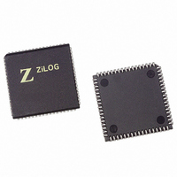
Z16F2810VH20EG Zilog, Z16F2810VH20EG Datasheet - Page 29

Z16F2810VH20EG
Manufacturer Part Number
Z16F2810VH20EG
Description
IC ZNEO MCU FLASH 128K 68PLCC
Manufacturer
Zilog
Series
Encore!® ZNEOr
Datasheet
1.Z16F2800100ZCOG.pdf
(388 pages)
Specifications of Z16F2810VH20EG
Core Processor
ZNEO
Core Size
16-Bit
Speed
20MHz
Connectivity
I²C, IrDA, LIN, SPI, UART/USART
Peripherals
Brown-out Detect/Reset, DMA, POR, PWM, WDT
Number Of I /o
46
Program Memory Size
128KB (128K x 8)
Program Memory Type
FLASH
Ram Size
4K x 8
Voltage - Supply (vcc/vdd)
2.7 V ~ 3.6 V
Data Converters
A/D 12x10b
Oscillator Type
Internal
Operating Temperature
-40°C ~ 105°C
Package / Case
68-LCC (J-Lead)
Data Bus Width
16 bit
Data Ram Size
4 B
Interface Type
ESPI, I2C, UART
Maximum Clock Frequency
20 MHz
Number Of Programmable I/os
46
Number Of Timers
4
Operating Supply Voltage
2.7 V to 3.6 V
Maximum Operating Temperature
+ 105 C
Mounting Style
SMD/SMT
Minimum Operating Temperature
- 40 C
On-chip Adc
10 bit, 12 Channel
For Use With
770-1003 - ISP 4PORT FOR ZILOG ZNEO MCU269-4537 - DEV KIT FOR Z16F ZNEO
Lead Free Status / RoHS Status
Lead free / RoHS Compliant
Eeprom Size
-
Lead Free Status / Rohs Status
Details
Other names
269-4691-5
Z16F2810VH20EG
Z16F2810VH20EG
Available stocks
Company
Part Number
Manufacturer
Quantity
Price
Company:
Part Number:
Z16F2810VH20EG
Manufacturer:
Zilog
Quantity:
151
- Current page: 29 of 388
- Download datasheet (22Mb)
Table 2. Signal Descriptions (Continued)
PS022008-0810
Signal Mnemonic
MISO
UART Controllers
TXD0/TXD1
RXD0/RXD1
CTS0/CTS1
DE0/DE1
General-Purpose Timers
T0OUT/T0OUT
T1OUT/T1OUT
T2OUT/T2OUT
T0IN/T0IN1/T0IN2
/T1IN/T2IN
Pulse-Width Modulator for Motor Control
PWMH0/PWMH1/
PWMH2
PWML0/PWML1/
PWML2
FAULT0/FAULTY
Analog
ANA[11:0]
VREF
Caution:
I/O
I/O
O
O
O
O
O
I
I
I
I
I
I
Description
Master-In/Slave-Out: This pin is the data input to the SPI mast er
device and the data output from the SPI slave device.
Transmit data: These signals transmit outputs from the UARTs.
Receive data: These signals receives inputs for the UARTs and
IrDAs.
Clear to Send: These signals are control inputs for the UARTs.
Driver enable (DE): This s ignal allows automatic control of
external RS-485 drivers. This signal is ap proximately the inverse
of the Transmit Empty ( TXE) bit in the UART Status 0 Re gister.
The DE sign al is used to ensure an external RS-485 driver is
enabled when data is transmitted by the UART.
General-purpose timer outputs: These signals are output pins
from the timers.
General-purpose timer inputs: These signals are used as the
capture, gating, and counter inputs.
PWM High output.
PWM Low output.
PWM Fault condition input: FAULT0 and FAULTY are active
Low.
Analog input: These signals are inputs to the ADC.
ADC reference voltage input or internal reference output:
The VREF pin must be capacitively coupled to analog ground, if
the internal voltage reference is selected as the ADC reference
voltage. A 10 mF capacitor is recommended.
P R E L I M I N A R Y
Signal and Pin Descriptions
Product Specification
ZNEO
Z16F Series
14
Related parts for Z16F2810VH20EG
Image
Part Number
Description
Manufacturer
Datasheet
Request
R

Part Number:
Description:
Communication Controllers, ZILOG INTELLIGENT PERIPHERAL CONTROLLER (ZIP)
Manufacturer:
Zilog, Inc.
Datasheet:

Part Number:
Description:
KIT DEV FOR Z8 ENCORE 16K TO 64K
Manufacturer:
Zilog
Datasheet:

Part Number:
Description:
KIT DEV Z8 ENCORE XP 28-PIN
Manufacturer:
Zilog
Datasheet:

Part Number:
Description:
DEV KIT FOR Z8 ENCORE 8K/4K
Manufacturer:
Zilog
Datasheet:

Part Number:
Description:
KIT DEV Z8 ENCORE XP 28-PIN
Manufacturer:
Zilog
Datasheet:

Part Number:
Description:
DEV KIT FOR Z8 ENCORE 4K TO 8K
Manufacturer:
Zilog
Datasheet:

Part Number:
Description:
CMOS Z8 microcontroller. ROM 16 Kbytes, RAM 256 bytes, speed 16 MHz, 32 lines I/O, 3.0V to 5.5V
Manufacturer:
Zilog, Inc.
Datasheet:

Part Number:
Description:
Low-cost microcontroller. 512 bytes ROM, 61 bytes RAM, 8 MHz
Manufacturer:
Zilog, Inc.
Datasheet:

Part Number:
Description:
Z8 4K OTP Microcontroller
Manufacturer:
Zilog, Inc.
Datasheet:

Part Number:
Description:
CMOS SUPER8 ROMLESS MCU
Manufacturer:
Zilog, Inc.
Datasheet:

Part Number:
Description:
SL1866 CMOSZ8 OTP Microcontroller
Manufacturer:
Zilog, Inc.
Datasheet:

Part Number:
Description:
SL1866 CMOSZ8 OTP Microcontroller
Manufacturer:
Zilog, Inc.
Datasheet:

Part Number:
Description:
OTP (KB) = 1, RAM = 125, Speed = 12, I/O = 14, 8-bit Timers = 2, Comm Interfaces Other Features = Por, LV Protect, Voltage = 4.5-5.5V
Manufacturer:
Zilog, Inc.
Datasheet:

Part Number:
Description:
Manufacturer:
Zilog, Inc.
Datasheet:


