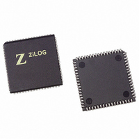
Z16F2810VH20EG Zilog, Z16F2810VH20EG Datasheet - Page 326

Z16F2810VH20EG
Manufacturer Part Number
Z16F2810VH20EG
Description
IC ZNEO MCU FLASH 128K 68PLCC
Manufacturer
Zilog
Series
Encore!® ZNEOr
Datasheet
1.Z16F2800100ZCOG.pdf
(388 pages)
Specifications of Z16F2810VH20EG
Core Processor
ZNEO
Core Size
16-Bit
Speed
20MHz
Connectivity
I²C, IrDA, LIN, SPI, UART/USART
Peripherals
Brown-out Detect/Reset, DMA, POR, PWM, WDT
Number Of I /o
46
Program Memory Size
128KB (128K x 8)
Program Memory Type
FLASH
Ram Size
4K x 8
Voltage - Supply (vcc/vdd)
2.7 V ~ 3.6 V
Data Converters
A/D 12x10b
Oscillator Type
Internal
Operating Temperature
-40°C ~ 105°C
Package / Case
68-LCC (J-Lead)
Data Bus Width
16 bit
Data Ram Size
4 B
Interface Type
ESPI, I2C, UART
Maximum Clock Frequency
20 MHz
Number Of Programmable I/os
46
Number Of Timers
4
Operating Supply Voltage
2.7 V to 3.6 V
Maximum Operating Temperature
+ 105 C
Mounting Style
SMD/SMT
Minimum Operating Temperature
- 40 C
On-chip Adc
10 bit, 12 Channel
For Use With
770-1003 - ISP 4PORT FOR ZILOG ZNEO MCU269-4537 - DEV KIT FOR Z16F ZNEO
Lead Free Status / RoHS Status
Lead free / RoHS Compliant
Eeprom Size
-
Lead Free Status / Rohs Status
Details
Other names
269-4691-5
Z16F2810VH20EG
Z16F2810VH20EG
Available stocks
Company
Part Number
Manufacturer
Quantity
Price
Company:
Part Number:
Z16F2810VH20EG
Manufacturer:
Zilog
Quantity:
151
- Current page: 326 of 388
- Download datasheet (22Mb)
PS022008-0810
On-Chip Debugger Commands
The hardware OCD supports several commands for controlling the device. In the
following list of commands, data sent from the host to the OCD is identified by
‘
Data
•
•
•
•
•
•
DBG <-- Data
Read Status Register — The Read Status register command returns the contents of the
Read Control Register — The Read Control register command returns the contents of
Read Registers — The Read registers command returns the contents of CPU registers
Read Revision — The Read Revision command returns the revision identifier.
OCDSTAT
the
Write Control Register — The Write Control register command writes data to the
OCDCTL
R15 through R0.
Write Registers — The Write registers command writes data to CPU registers R15
through R0.
’. Multiple bytes transmitted are represented with double arrows ‘<<‘or’>>’.
OCDCTL
DBG <-- 0000_0000
DBG --> RevID[15:8]
DBG --> RevID[7:0]
DBG --> CRC[0:7]
DBG <-- 0000_0001
DBG --> status[7:0]
DBG --> CRC[0:7]
DBG <-- 0000_0010
DBG --> OCDCTL[7:0]
DBG --> CRC[0:7]
DBG <-- 0000_0011
DBG <-- OCDCTL[7:0]
DBG --> CRC[0:7]
DBG <-- 0000_0100
DBG ->> regdata[31:24]
DBG ->> regdata[23:16]
DBG ->> regdata[15:8]
DBG ->> regdata[7:0]
DBG --> CRC[0:7]
DBG <-- 0000_0101
DBG <<- regdata[31:24]
DBG <<- regdata[23:16]
DBG <<- regdata[15:8]
DBG <<- regdata[7:0]
DBG --> CRC[0:7]
register.
register.
register.
’. Data sent from the OCD back to the host is identified by ‘
P R E L I M I N A R Y
Product Specification
ZNEO
On-Chip Debugger
Z16F Series
DBG -->
310
Related parts for Z16F2810VH20EG
Image
Part Number
Description
Manufacturer
Datasheet
Request
R

Part Number:
Description:
Communication Controllers, ZILOG INTELLIGENT PERIPHERAL CONTROLLER (ZIP)
Manufacturer:
Zilog, Inc.
Datasheet:

Part Number:
Description:
KIT DEV FOR Z8 ENCORE 16K TO 64K
Manufacturer:
Zilog
Datasheet:

Part Number:
Description:
KIT DEV Z8 ENCORE XP 28-PIN
Manufacturer:
Zilog
Datasheet:

Part Number:
Description:
DEV KIT FOR Z8 ENCORE 8K/4K
Manufacturer:
Zilog
Datasheet:

Part Number:
Description:
KIT DEV Z8 ENCORE XP 28-PIN
Manufacturer:
Zilog
Datasheet:

Part Number:
Description:
DEV KIT FOR Z8 ENCORE 4K TO 8K
Manufacturer:
Zilog
Datasheet:

Part Number:
Description:
CMOS Z8 microcontroller. ROM 16 Kbytes, RAM 256 bytes, speed 16 MHz, 32 lines I/O, 3.0V to 5.5V
Manufacturer:
Zilog, Inc.
Datasheet:

Part Number:
Description:
Low-cost microcontroller. 512 bytes ROM, 61 bytes RAM, 8 MHz
Manufacturer:
Zilog, Inc.
Datasheet:

Part Number:
Description:
Z8 4K OTP Microcontroller
Manufacturer:
Zilog, Inc.
Datasheet:

Part Number:
Description:
CMOS SUPER8 ROMLESS MCU
Manufacturer:
Zilog, Inc.
Datasheet:

Part Number:
Description:
SL1866 CMOSZ8 OTP Microcontroller
Manufacturer:
Zilog, Inc.
Datasheet:

Part Number:
Description:
SL1866 CMOSZ8 OTP Microcontroller
Manufacturer:
Zilog, Inc.
Datasheet:

Part Number:
Description:
OTP (KB) = 1, RAM = 125, Speed = 12, I/O = 14, 8-bit Timers = 2, Comm Interfaces Other Features = Por, LV Protect, Voltage = 4.5-5.5V
Manufacturer:
Zilog, Inc.
Datasheet:

Part Number:
Description:
Manufacturer:
Zilog, Inc.
Datasheet:


