M30833FJFP#U5 Renesas Electronics America, M30833FJFP#U5 Datasheet - Page 189
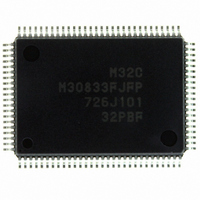
M30833FJFP#U5
Manufacturer Part Number
M30833FJFP#U5
Description
IC M32C/83 MCU FLASH 100QFP
Manufacturer
Renesas Electronics America
Series
M16C™ M32C/80r
Datasheets
1.M3087BFLGPU3.pdf
(364 pages)
2.M30833FJGPU3.pdf
(96 pages)
3.M30833FJGPU3.pdf
(529 pages)
Specifications of M30833FJFP#U5
Core Processor
M32C/80
Core Size
16/32-Bit
Speed
32MHz
Connectivity
CAN, I²C, IEBus, SIO, UART/USART
Peripherals
DMA, WDT
Number Of I /o
85
Program Memory Size
512KB (512K x 8)
Program Memory Type
FLASH
Ram Size
31K x 8
Voltage - Supply (vcc/vdd)
3 V ~ 5.5 V
Data Converters
A/D 26x10b; D/A 2x8b
Oscillator Type
Internal
Operating Temperature
-20°C ~ 85°C
Package / Case
100-QFP
For Use With
R0K330879S001BE - KIT DEV RSK M32C/87R0K330879S000BE - KIT DEV RSK M32C/87
Lead Free Status / RoHS Status
Lead free / RoHS Compliant
Eeprom Size
-
Available stocks
Company
Part Number
Manufacturer
Quantity
Price

Part Number:
M30833FJFP#U5M30833FJFP#U3
Manufacturer:
Renesas Electronics America
Quantity:
135
Part Number:
M30833FJFP#U5M30833FJFP#U3
Manufacturer:
Renesas Electronics America
Quantity:
10 000


M
R
R
e
E
3
. v
J
2
Figure 15.2 INVC0 Register
0
C
1
9
3 .
8 /
B
0
1
3
0
3
G
NOTES:
J
Timing to Transfer from the IDB0
and IDB1 Registers to Three-Phase
Output Shift Register
Timing to Trigger the Dead Time
Timer when the INV16 Bit=0
INV13 Bit
4
a
Mode
Transfer trigger : Timer B2 underflows and write to the INV07 bit, or write to the TB2 register when INV10 = 1
o r
0 -
n
Three-Phase PWM Control Register 0
10. When the INV06 bit is set to "1", set the INV11 bit to "0" (three-phase mode 0) and the PWCON bit in the
1. Set the INVC0 register after the PRC1 bit in the PRCR register is set to "1" (write enable).
2. Set the INV01 bit to "1" after setting the ICTB2 register .
3. The INV00 and INV01 bits are enabled only when the INV11 bit is set to "1" (three-phase mode 1). The ICTB2
4. Set the INV02 bit to "1" to operate the dead time timer, U-, V-and W-phase output control circuits and the ICTB2
5. Set pins after the INV02 bit is set to "1". See Table 15.2 for pin settings.
6. When the INV02 bit is set to "1" and the INV03 bit to "0", U, U, V, V, W and W pins, including pins shared with
7. The INV03 bit is set to "0" when the followings occurs :
8. The INV05 bit can not be set to "1" by program. Set the INV04 bit to "0", as well, when setting the INV05 bit to "0".
9. The following table describes how the INV06 bit works.
b7
3 .
u
1
TB2SC register to "0" (timer B2 counter underflows).
When setting the INV01 bit to "1", set the timer A1 count start flag before the first timer B2 counter underflow.
Rewrite the INV00 to INV02 and INV06 bits when the timers A1,A2, A4 and B2 stop.
counter is incremented by one every time the timer B2 counter underflows, regardless of INV00 and INV01 bit
settings, when the INV11 bit is set to "0" (three-phase mode).
When the INV00 bit is set to "1", the first interrupt is generated when the timer B2 counter underflows n-1 times,
if n is the value set in the ICTB2 counter. Subsequent interrupts are generated every n times the timer B2
counter underflows.
counter.
other output functions, are placed in high-impedance states.
p
, 1
3
b6
1
- Reset
- A concurrent active state occurs while INV04 bit is set to "1"
- The INV03 bit is set to "0" by program
- A signal applied to the NMI pin changes "H" to "L"
(
2
M
b5
0
3
0
2
6
b4
C
Item
8 /
b3
Page 164
, 3
b2
M
b1
3
2
b0
C
f o
8 /
Symbol
INV00
INV01
INV02
INV03
INV04
INV05
INV06
INV07
4
3
8
) T
Bit
8
Symbol
INVC0
Triangular wave modulation mode
Transferred once by generating a
transfer trigger after setting the IDB0
and IDB1 registers
On the falling edge of a one-shot pulse
of the timer A1, A2 or A4
Enabled when the INV11 bit=1 and the
INV06 bit=0
Interrupt Enable Output
Polarity Select Bit
Interrupt Enable Output
Specification Bit
Mode Select Bit
Output Control Bit
Positive and Negative-
Phases Concurrent Active
Disable Function Enable Bit
Positive and Negative-
Phases Concurrent Active
Output Detect Flag
Modulation Mode
Select
Software Trigger Select
(9, 10)
Bit Name
INV06 = 0
Address
0308
(4, 5, 6)
(2, 3)
(8)
(3)
16
(6, 7)
(1)
0: The ICTB2 counter is incremented by one on the
1: The ICTB2 counter is incremented by one on the
0: ICTB2 counter is incremented by one
1: Selected by the INV00 bit
0: No three-phase control timer functions
1: Three-phase control timer function
0: Disables three-phase control timer output
1: Enables three-phase control timer output
0: Enables concurrent active output
1: Disables concurrent active output
0: Not detected
1: Detected
0: Triangular wave modulation mode
1: Sawtooth wave modulation mode
Transfer trigger is generated when the
INV07 bit is set to "1". Trigger to the dead
time timer is also generated when setting the
INV06 bit to "1". Its value is "0" when read.
15. Three-Phase Motor Control Timer Functions
rising edge of the timer A1 reload control signal
falling edge of the timer A1 reload control signal
whenever the timer B2 counter underflows
Sawtooth wave modulation mode
Transferred every time a transfer trigger
is generated
By a transfer trigger, or the falling edge of
a one-shot pulse of the timer A1, A2 or A4
Disabled
After Reset
00
16
Function
INV06 = 1
RW
RW
RW
RW
RW
RW
RW
RW
RW
Related parts for M30833FJFP#U5
Image
Part Number
Description
Manufacturer
Datasheet
Request
R

Part Number:
Description:
KIT STARTER FOR M16C/29
Manufacturer:
Renesas Electronics America
Datasheet:

Part Number:
Description:
KIT STARTER FOR R8C/2D
Manufacturer:
Renesas Electronics America
Datasheet:

Part Number:
Description:
R0K33062P STARTER KIT
Manufacturer:
Renesas Electronics America
Datasheet:

Part Number:
Description:
KIT STARTER FOR R8C/23 E8A
Manufacturer:
Renesas Electronics America
Datasheet:

Part Number:
Description:
KIT STARTER FOR R8C/25
Manufacturer:
Renesas Electronics America
Datasheet:

Part Number:
Description:
KIT STARTER H8S2456 SHARPE DSPLY
Manufacturer:
Renesas Electronics America
Datasheet:

Part Number:
Description:
KIT STARTER FOR R8C38C
Manufacturer:
Renesas Electronics America
Datasheet:

Part Number:
Description:
KIT STARTER FOR R8C35C
Manufacturer:
Renesas Electronics America
Datasheet:

Part Number:
Description:
KIT STARTER FOR R8CL3AC+LCD APPS
Manufacturer:
Renesas Electronics America
Datasheet:
Part Number:
Description:
KIT STARTER FOR RX610
Manufacturer:
Renesas Electronics America
Datasheet:

Part Number:
Description:
KIT STARTER FOR R32C/118
Manufacturer:
Renesas Electronics America
Datasheet:

Part Number:
Description:
KIT DEV RSK-R8C/26-29
Manufacturer:
Renesas Electronics America
Datasheet:

Part Number:
Description:
KIT STARTER FOR SH7124
Manufacturer:
Renesas Electronics America
Datasheet:

Part Number:
Description:
KIT STARTER FOR H8SX/1622
Manufacturer:
Renesas Electronics America
Datasheet:

Part Number:
Description:
KIT DEV FOR SH7203
Manufacturer:
Renesas Electronics America
Datasheet: