M30833FJFP#U5 Renesas Electronics America, M30833FJFP#U5 Datasheet - Page 351
M30833FJFP#U5
Manufacturer Part Number
M30833FJFP#U5
Description
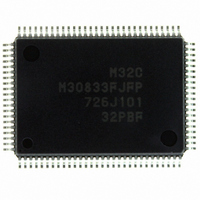
IC M32C/83 MCU FLASH 100QFP
Manufacturer
Renesas Electronics America
Series
M16C™ M32C/80r
Datasheets
1.M3087BFLGPU3.pdf
(364 pages)
2.M30833FJGPU3.pdf
(96 pages)
3.M30833FJGPU3.pdf
(529 pages)
Specifications of M30833FJFP#U5
Core Processor
M32C/80
Core Size
16/32-Bit
Speed
32MHz
Connectivity
CAN, I²C, IEBus, SIO, UART/USART
Peripherals
DMA, WDT
Number Of I /o
85
Program Memory Size
512KB (512K x 8)
Program Memory Type
FLASH
Ram Size
31K x 8
Voltage - Supply (vcc/vdd)
3 V ~ 5.5 V
Data Converters
A/D 26x10b; D/A 2x8b
Oscillator Type
Internal
Operating Temperature
-20°C ~ 85°C
Package / Case
100-QFP
For Use With
R0K330879S001BE - KIT DEV RSK M32C/87R0K330879S000BE - KIT DEV RSK M32C/87
Lead Free Status / RoHS Status
Lead free / RoHS Compliant
Eeprom Size
-
Available stocks
Company
Part Number
Manufacturer
Quantity
Price

Part Number:
M30833FJFP#U5M30833FJFP#U3
Manufacturer:
Renesas Electronics America
Quantity:
135
Part Number:
M30833FJFP#U5M30833FJFP#U3
Manufacturer:
Renesas Electronics America
Quantity:
10 000


R
R
M
e
E
3
. v
J
Figure 22.3 C0CTLR0 Register
2
0
1
C
22.1 CAN-Associated Registers
22.1.1 CAN0 Control Register 0 (C0CTLR0 Register)
9
3 .
B
8 /
0
1
Figures 22.3 to 22.26 show registers associated with CAN. To access the associated registers, set the
MCD4 to MCD0 bits in the MCD register to "10010
register to "1" (2 wait states), and the CM07 bit in the CM0 register to "0" (X
3
0
3
J
G
b15
4
a
NOTES:
CAN0 Control Register 0
0 -
o r
n
3 .
1. Value is obtained by setting the SLEEP bit in the C0SLPR register to "1" (sleep mode exited) and
2. Set the RESET0 bit and RESET1 bit to the same value simultaneously.
3. This bit can be set to "1" by program, but cannot be set to "0".
1
u
, 1
3
p
supplying a clock to the CAN module after reset.
1
(
2
M
0
0
3
6
2
b8
C
b7
8 /
Page 326
, 3
0
M
3
2
C
b0
f o
8 /
(b15 - b12)
LOOPBACK
BASICCAN
ECRESET
TSRESET
4
Symbol
RESET0
RESET1
(b7 - b6)
TSPRE0
TSPRE1
3
8
(b2)
(b5)
) T
Bit
8
Symbol
C0CTLR0
CAN Reset Bit 0
Loop Back Mode
Select Bit
Basic CAN Mode
Select Bit
CAN Reset Bit 1
Reserved Bit
Nothing is assigned. When write, set to "0".
When read, its content is indeterminate.
Time Stamp
Prescaler Select Bit
Time Stamp
Counter Reset Bit
Error Counter
Reset Bit
Nothing is assigned. When write, set to "0".
When read, its content is indeterminate.
Nothing is assigned. When write, set to "0".
When read, its content is indeterminate.
Bit Name
Address
0201
16
2
- 0200
" (no division of CPU clock), the PM13 bit in the PM1
0: CAN module reset exited
1: CAN module is reset
0: Disables Loop back function
1: Enables Loop back function
0 : Disables BasicCAN mode function
1 : Enables BasicCAN mode function
0: CAN module reset exited
1: CAN module is reset
Set to "0".
b9 b8
0 0: Selects the CAN bus bit clock
0 1: Selects the CAN bus bit clock divided by 2
1 0: Selects the CAN bus bit clock divided by 3
1 1: Selects the CAN bus bit clock divided by 4
When this bit is set to "1", the C0TSR
register is set to "0000
this bit is automatically set to "0".
When this bit is set to "1", the C0TEC
and C0REC registers are set to "00
After that, this bit is automatically set to "0".
16
After Reset
XXXX 0000 XX01 0X01
Function
16
(2)
(2)
". After that,
IN
(1)
-X
OUT
(3)
16
".
selected).
2
(3)
22. CAN Module
RW
RW
RW
RW
RW
RW
RW
RW
RW
RW
Related parts for M30833FJFP#U5
Image
Part Number
Description
Manufacturer
Datasheet
Request
R

Part Number:
Description:
KIT STARTER FOR M16C/29
Manufacturer:
Renesas Electronics America
Datasheet:

Part Number:
Description:
KIT STARTER FOR R8C/2D
Manufacturer:
Renesas Electronics America
Datasheet:

Part Number:
Description:
R0K33062P STARTER KIT
Manufacturer:
Renesas Electronics America
Datasheet:

Part Number:
Description:
KIT STARTER FOR R8C/23 E8A
Manufacturer:
Renesas Electronics America
Datasheet:

Part Number:
Description:
KIT STARTER FOR R8C/25
Manufacturer:
Renesas Electronics America
Datasheet:

Part Number:
Description:
KIT STARTER H8S2456 SHARPE DSPLY
Manufacturer:
Renesas Electronics America
Datasheet:

Part Number:
Description:
KIT STARTER FOR R8C38C
Manufacturer:
Renesas Electronics America
Datasheet:

Part Number:
Description:
KIT STARTER FOR R8C35C
Manufacturer:
Renesas Electronics America
Datasheet:

Part Number:
Description:
KIT STARTER FOR R8CL3AC+LCD APPS
Manufacturer:
Renesas Electronics America
Datasheet:
Part Number:
Description:
KIT STARTER FOR RX610
Manufacturer:
Renesas Electronics America
Datasheet:

Part Number:
Description:
KIT STARTER FOR R32C/118
Manufacturer:
Renesas Electronics America
Datasheet:

Part Number:
Description:
KIT DEV RSK-R8C/26-29
Manufacturer:
Renesas Electronics America
Datasheet:

Part Number:
Description:
KIT STARTER FOR SH7124
Manufacturer:
Renesas Electronics America
Datasheet:

Part Number:
Description:
KIT STARTER FOR H8SX/1622
Manufacturer:
Renesas Electronics America
Datasheet:

Part Number:
Description:
KIT DEV FOR SH7203
Manufacturer:
Renesas Electronics America
Datasheet: