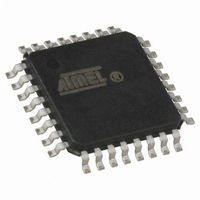
AT89LP428-20AU Atmel, AT89LP428-20AU Datasheet - Page 81

AT89LP428-20AU
Manufacturer Part Number
AT89LP428-20AU
Description
MCU 8051 4K FLASH SPI 32TQFP
Manufacturer
Atmel
Series
89LPr
Datasheet
1.AT89LP428-20AU.pdf
(149 pages)
Specifications of AT89LP428-20AU
Core Processor
8051
Core Size
8-Bit
Speed
20MHz
Connectivity
SPI, UART/USART
Peripherals
Brown-out Detect/Reset, POR, PWM, WDT
Number Of I /o
30
Program Memory Size
4KB (4K x 8)
Program Memory Type
FLASH
Eeprom Size
512 x 8
Ram Size
768 x 8
Voltage - Supply (vcc/vdd)
2.4 V ~ 5.5 V
Oscillator Type
Internal
Operating Temperature
-40°C ~ 85°C
Package / Case
32-TQFP, 32-VQFP
Processor Series
AT89x
Core
8051
3rd Party Development Tools
PK51, CA51, A51, ULINK2
Development Tools By Supplier
AT89ISP
Lead Free Status / RoHS Status
Lead free / RoHS Compliant
Data Converters
-
Lead Free Status / Rohs Status
Details
Available stocks
Company
Part Number
Manufacturer
Quantity
Price
Company:
Part Number:
AT89LP428-20AU
Manufacturer:
RFMD
Quantity:
1 240
16.3
3654A–MICRO–8/09
More About Mode 0
Table 16-3.
In Mode 0, the UART is configured as a 2-wire half-duplex synchronous serial interface. Serial
data enters and exits through RXD. TXD outputs the shift clock. Eight data bits are transmit-
ted/received, with the LSB first.
the serial port in Mode 0 and associated timing. The baud rate is programmable to 1/2 or 1/4 the
oscillator frequency by setting/clearing the SMOD1 bit. However, changing SMOD1 has an
effect on the relationship between the clock and data as described below. The baud rate can
also be generated by Timer 1 by setting TB8.
Table 16-4.
Transmission is initiated by any instruction that uses SBUF as a destination register. The “write
to SBUF” signal also loads a “1” into the 9th position of the transmit shift register and tells the TX
Control Block to begin a transmission. The internal timing is such that one full bit slot may elapse
between “write to SBUF” and activation of SEND.
SEND transfers the output of the shift register to the alternate output function line of P3.0, and
also transfers Shift Clock to the alternate output function line of P3.1. As data bits shift out to the
right, “0”s come in from the left. When the MSB of the data byte is at the output position of the
shift register, the “1” that was initially loaded into the 9th position is just to the left of the MSB,
and all positions to the left of that contain “0”s. This condition flags the TX Control block to do
one last shift, then deactivate SEND and set TI.
Baud Rate
TB8
62.5K
19.2K
137.5
9.6K
4.8K
2.4K
1.2K
110
110
0
0
1
1
Commonly Used Baud Rates Generated by Timer 2 (TPS = 0000B)
Mode 0 Baud Rates
SMOD1
f
OSC
11.059
11.059
11.059
11.059
11.059
11.986
0
1
0
1
12
12
(MHz)
6
Figure 16-1 on page 83
CP/RL2
0
0
0
0
0
0
0
0
0
Table 16-4
C/T2
0
0
0
0
0
0
0
0
0
shows a simplified functional diagram of
(Timer 1 Overflow)/4
(Timer 1 Overflow)/2
lists the baud rate options for Mode 0.
Baud Rate
TCLK or RCLK
f
f
Timer 2
SYS
SYS
AT89LP428/828
/4
/2
1
1
1
1
1
1
1
1
1
Reload Value
FFDCH
FDC0H
FEE0H
EAB8H
FFF4H
FFB8H
FF70H
F2AFH
E55EH
81


