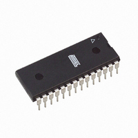
ATMEGA8L-8PU Atmel, ATMEGA8L-8PU Datasheet - Page 143

ATMEGA8L-8PU
Manufacturer Part Number
ATMEGA8L-8PU
Description
IC AVR MCU 8K 8MHZ 3V 28DIP
Manufacturer
Atmel
Series
AVR® ATmegar
Datasheets
1.ATMEGA8L-8MU.pdf
(25 pages)
2.ATMEGA8L-8MU.pdf
(302 pages)
3.ATMEGA8-16PU.pdf
(305 pages)
Specifications of ATMEGA8L-8PU
Core Processor
AVR
Core Size
8-Bit
Speed
8MHz
Connectivity
I²C, SPI, UART/USART
Peripherals
Brown-out Detect/Reset, POR, PWM, WDT
Number Of I /o
23
Program Memory Size
8KB (4K x 16)
Program Memory Type
FLASH
Eeprom Size
512 x 8
Ram Size
1K x 8
Voltage - Supply (vcc/vdd)
2.7 V ~ 5.5 V
Data Converters
A/D 6x10b
Oscillator Type
Internal
Operating Temperature
-40°C ~ 85°C
Package / Case
28-DIP (0.300", 7.62mm)
Cpu Family
ATmega
Device Core
AVR
Device Core Size
8b
Frequency (max)
8MHz
Interface Type
SPI/TWI/USART
Total Internal Ram Size
1KB
# I/os (max)
23
Number Of Timers - General Purpose
3
Operating Supply Voltage (typ)
3.3/5V
Operating Supply Voltage (max)
5.5V
Operating Supply Voltage (min)
2.7V
On-chip Adc
6-chx10-bit
Instruction Set Architecture
RISC
Operating Temp Range
-40C to 85C
Operating Temperature Classification
Industrial
Mounting
Through Hole
Pin Count
28
Package Type
PDIP
Processor Series
ATMEGA8x
Core
AVR8
Data Bus Width
8 bit
Data Ram Size
1 KB
Maximum Clock Frequency
8 MHz
Number Of Programmable I/os
23
Number Of Timers
3
Operating Supply Voltage
2.7 V to 5.5 V
Maximum Operating Temperature
+ 85 C
Mounting Style
Through Hole
3rd Party Development Tools
EWAVR, EWAVR-BL
Minimum Operating Temperature
- 40 C
Controller Family/series
AVR MEGA
No. Of I/o's
23
Eeprom Memory Size
512Byte
Ram Memory Size
1KB
Cpu Speed
8MHz
Rohs Compliant
Yes
For Use With
ATSTK600-TQFP32 - STK600 SOCKET/ADAPTER 32-TQFPATSTK600-DIP40 - STK600 SOCKET/ADAPTER 40-PDIP770-1007 - ISP 4PORT ATMEL AVR MCU SPI/JTAGATAVRISP2 - PROGRAMMER AVR IN SYSTEMATSTK500 - PROGRAMMER AVR STARTER KIT
Lead Free Status / RoHS Status
Lead free / RoHS Compliant
Available stocks
Company
Part Number
Manufacturer
Quantity
Price
Company:
Part Number:
ATMEGA8L-8PU
Manufacturer:
BROADCOM
Quantity:
101
Company:
Part Number:
ATMEGA8L-8PU
Manufacturer:
ATMEL
Quantity:
33 600
Part Number:
ATMEGA8L-8PU
Manufacturer:
ATMEL/爱特梅尔
Quantity:
20 000
Company:
Part Number:
ATMEGA8L-8PU-QS096
Manufacturer:
ATMEL
Quantity:
56
Asynchronous Data
Recovery
2486Z–AVR–02/11
the figure. The clock recovery logic then uses samples 8, 9 and 10 for Normal mode, and
samples 4, 5 and 6 for Double Speed mode (indicated with sample numbers inside boxes on the
figure), to decide if a valid start bit is received. If two or more of these three samples have logical
high levels (the majority wins), the start bit is rejected as a noise spike and the Receiver starts
looking for the next high to low-transition. If however, a valid start bit is detected, the clock
recovery logic is synchronized and the data recovery can begin. The synchronization process is
repeated for each start bit.
When the Receiver clock is synchronized to the start bit, the data recovery can begin. The data
recovery unit uses a state machine that has 16 states for each bit in Normal mode and eight
states for each bit in Double Speed mode.
parity bit. Each of the samples is given a number that is equal to the state of the recovery unit.
Figure 66. Sampling of Data and Parity Bit
The decision of the logic level of the received bit is taken by doing a majority voting of the logic
value to the three samples in the center of the received bit. The center samples are emphasized
on the figure by having the sample number inside boxes. The majority voting process is done as
follows: If two or all three samples have high levels, the received bit is registered to be a logic 1.
If two or all three samples have low levels, the received bit is registered to be a logic 0. This
majority voting process acts as a low pass filter for the incoming signal on the RxD pin. The
recovery process is then repeated until a complete frame is received. Including the first stop bit.
Note that the Receiver only uses the first stop bit of a frame.
Figure 67
the next frame.
Figure 67. Stop Bit Sampling and Next Start Bit Sampling
The same majority voting is done to the stop bit as done for the other bits in the frame. If the stop
bit is registered to have a logic 0 value, the Frame Error (FE) Flag will be set.
A new high to low transition indicating the start bit of a new frame can come right after the last of
the bits used for majority voting. For Normal Speed mode, the first low level sample can be at
point marked (A) in
(C) marks a stop bit of full length. The early start bit detection influences the operational range of
the Receiver.
(U2X = 0)
(U2X = 1)
(U2X = 0)
(U2X = 1)
Sample
Sample
Sample
Sample
RxD
RxD
shows the sampling of the stop bit and the earliest possible beginning of the start bit of
Figure
1
1
1
1
2
2
67. For Double Speed mode the first low level must be delayed to (B).
3
2
3
2
4
4
5
3
5
3
6
6
Figure 66
7
4
7
4
8
8
STOP 1
BIT n
9
5
9
5
shows the sampling of the data bits and the
10
10
(A)
0/1
11
6
6
0/1
12
(B)
0/1
0/1
13
7
14
ATmega8(L)
15
8
16
(C)
1
1
143


