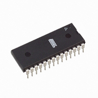
ATMEGA8L-8PU Atmel, ATMEGA8L-8PU Datasheet - Page 91

ATMEGA8L-8PU
Manufacturer Part Number
ATMEGA8L-8PU
Description
IC AVR MCU 8K 8MHZ 3V 28DIP
Manufacturer
Atmel
Series
AVR® ATmegar
Datasheets
1.ATMEGA8L-8MU.pdf
(25 pages)
2.ATMEGA8L-8MU.pdf
(302 pages)
3.ATMEGA8-16PU.pdf
(305 pages)
Specifications of ATMEGA8L-8PU
Core Processor
AVR
Core Size
8-Bit
Speed
8MHz
Connectivity
I²C, SPI, UART/USART
Peripherals
Brown-out Detect/Reset, POR, PWM, WDT
Number Of I /o
23
Program Memory Size
8KB (4K x 16)
Program Memory Type
FLASH
Eeprom Size
512 x 8
Ram Size
1K x 8
Voltage - Supply (vcc/vdd)
2.7 V ~ 5.5 V
Data Converters
A/D 6x10b
Oscillator Type
Internal
Operating Temperature
-40°C ~ 85°C
Package / Case
28-DIP (0.300", 7.62mm)
Cpu Family
ATmega
Device Core
AVR
Device Core Size
8b
Frequency (max)
8MHz
Interface Type
SPI/TWI/USART
Total Internal Ram Size
1KB
# I/os (max)
23
Number Of Timers - General Purpose
3
Operating Supply Voltage (typ)
3.3/5V
Operating Supply Voltage (max)
5.5V
Operating Supply Voltage (min)
2.7V
On-chip Adc
6-chx10-bit
Instruction Set Architecture
RISC
Operating Temp Range
-40C to 85C
Operating Temperature Classification
Industrial
Mounting
Through Hole
Pin Count
28
Package Type
PDIP
Processor Series
ATMEGA8x
Core
AVR8
Data Bus Width
8 bit
Data Ram Size
1 KB
Maximum Clock Frequency
8 MHz
Number Of Programmable I/os
23
Number Of Timers
3
Operating Supply Voltage
2.7 V to 5.5 V
Maximum Operating Temperature
+ 85 C
Mounting Style
Through Hole
3rd Party Development Tools
EWAVR, EWAVR-BL
Minimum Operating Temperature
- 40 C
Controller Family/series
AVR MEGA
No. Of I/o's
23
Eeprom Memory Size
512Byte
Ram Memory Size
1KB
Cpu Speed
8MHz
Rohs Compliant
Yes
For Use With
ATSTK600-TQFP32 - STK600 SOCKET/ADAPTER 32-TQFPATSTK600-DIP40 - STK600 SOCKET/ADAPTER 40-PDIP770-1007 - ISP 4PORT ATMEL AVR MCU SPI/JTAGATAVRISP2 - PROGRAMMER AVR IN SYSTEMATSTK500 - PROGRAMMER AVR STARTER KIT
Lead Free Status / RoHS Status
Lead free / RoHS Compliant
Available stocks
Company
Part Number
Manufacturer
Quantity
Price
Company:
Part Number:
ATMEGA8L-8PU
Manufacturer:
BROADCOM
Quantity:
101
Company:
Part Number:
ATMEGA8L-8PU
Manufacturer:
ATMEL
Quantity:
33 600
Part Number:
ATMEGA8L-8PU
Manufacturer:
ATMEL/爱特梅尔
Quantity:
20 000
Company:
Part Number:
ATMEGA8L-8PU-QS096
Manufacturer:
ATMEL
Quantity:
56
2486Z–AVR–02/11
tion. The diagram includes non-inverted and inverted PWM outputs. The small horizontal line
marks on the TCNT1 slopes represent compare matches between OCR1x and TCNT1. The
OC1x Interrupt Flag will be set when a Compare Match occurs.
Figure 39. Phase Correct PWM Mode, Timing Diagram
The Timer/Counter Overflow Flag (TOV1) is set each time the counter reaches BOTTOM. When
either OCR1A or ICR1 is used for defining the TOP value, the OC1A or ICF1 Flag is set accord-
ingly at the same timer clock cycle as the OCR1x Registers are updated with the double buffer
value (at TOP). The Interrupt Flags can be used to generate an interrupt each time the counter
reaches the TOP or BOTTOM value.
When changing the TOP value the program must ensure that the new TOP value is higher or
equal to the value of all of the Compare Registers. If the TOP value is lower than any of the
Compare Registers, a Compare Match will never occur between the TCNT1 and the OCR1x.
Note that when using fixed TOP values, the unused bits are masked to zero when any of the
OCR1x Registers are written. As the third period shown in
TOP actively while the Timer/Counter is running in the Phase Correct mode can result in an
unsymmetrical output. The reason for this can be found in the time of update of the OCR1x Reg-
ister. Since the OCR1x update occurs at TOP, the PWM period starts and ends at TOP. This
implies that the length of the falling slope is determined by the previous TOP value, while the
length of the rising slope is determined by the new TOP value. When these two values differ the
two slopes of the period will differ in length. The difference in length gives the unsymmetrical
result on the output.
It is recommended to use the Phase and Frequency Correct mode instead of the Phase Correct
mode when changing the TOP value while the Timer/Counter is running. When using a static
TOP value there are practically no differences between the two modes of operation.
In phase correct PWM mode, the compare units allow generation of PWM waveforms on the
OC1x pins. Setting the COM1x1:0 bits to 2 will produce a non-inverted PWM and an inverted
PWM output can be generated by setting the COM1x1:0 to 3. See
actual OC1x value will only be visible on the port pin if the data direction for the port pin is set as
output (DDR_OC1x). The PWM waveform is generated by setting (or clearing) the OC1x Regis-
ter at the Compare Match between OCR1x and TCNT1 when the counter increments, and
clearing (or setting) the OC1x Register at Compare Match between OCR1x and TCNT1 when
TCNTn
OCnx
OCnx
Period
1
2
3
Figure 39
Table 38 on page
4
OCRnx / TOP Update and
OCnA Interrupt Flag Set
or ICFn Interrupt Flag Set
(Interrupt on TOP)
illustrates, changing the
TOVn Interrupt Flag Set
(Interrupt on Bottom)
ATmega8(L)
(COMnx1:0 = 2)
(COMnx1:0 = 3)
97. The
91


