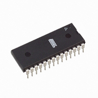
ATMEGA8L-8PU Atmel, ATMEGA8L-8PU Datasheet - Page 206

ATMEGA8L-8PU
Manufacturer Part Number
ATMEGA8L-8PU
Description
IC AVR MCU 8K 8MHZ 3V 28DIP
Manufacturer
Atmel
Series
AVR® ATmegar
Datasheets
1.ATMEGA8L-8MU.pdf
(25 pages)
2.ATMEGA8L-8MU.pdf
(302 pages)
3.ATMEGA8-16PU.pdf
(305 pages)
Specifications of ATMEGA8L-8PU
Core Processor
AVR
Core Size
8-Bit
Speed
8MHz
Connectivity
I²C, SPI, UART/USART
Peripherals
Brown-out Detect/Reset, POR, PWM, WDT
Number Of I /o
23
Program Memory Size
8KB (4K x 16)
Program Memory Type
FLASH
Eeprom Size
512 x 8
Ram Size
1K x 8
Voltage - Supply (vcc/vdd)
2.7 V ~ 5.5 V
Data Converters
A/D 6x10b
Oscillator Type
Internal
Operating Temperature
-40°C ~ 85°C
Package / Case
28-DIP (0.300", 7.62mm)
Cpu Family
ATmega
Device Core
AVR
Device Core Size
8b
Frequency (max)
8MHz
Interface Type
SPI/TWI/USART
Total Internal Ram Size
1KB
# I/os (max)
23
Number Of Timers - General Purpose
3
Operating Supply Voltage (typ)
3.3/5V
Operating Supply Voltage (max)
5.5V
Operating Supply Voltage (min)
2.7V
On-chip Adc
6-chx10-bit
Instruction Set Architecture
RISC
Operating Temp Range
-40C to 85C
Operating Temperature Classification
Industrial
Mounting
Through Hole
Pin Count
28
Package Type
PDIP
Processor Series
ATMEGA8x
Core
AVR8
Data Bus Width
8 bit
Data Ram Size
1 KB
Maximum Clock Frequency
8 MHz
Number Of Programmable I/os
23
Number Of Timers
3
Operating Supply Voltage
2.7 V to 5.5 V
Maximum Operating Temperature
+ 85 C
Mounting Style
Through Hole
3rd Party Development Tools
EWAVR, EWAVR-BL
Minimum Operating Temperature
- 40 C
Controller Family/series
AVR MEGA
No. Of I/o's
23
Eeprom Memory Size
512Byte
Ram Memory Size
1KB
Cpu Speed
8MHz
Rohs Compliant
Yes
For Use With
ATSTK600-TQFP32 - STK600 SOCKET/ADAPTER 32-TQFPATSTK600-DIP40 - STK600 SOCKET/ADAPTER 40-PDIP770-1007 - ISP 4PORT ATMEL AVR MCU SPI/JTAGATAVRISP2 - PROGRAMMER AVR IN SYSTEMATSTK500 - PROGRAMMER AVR STARTER KIT
Lead Free Status / RoHS Status
Lead free / RoHS Compliant
Available stocks
Company
Part Number
Manufacturer
Quantity
Price
Company:
Part Number:
ATMEGA8L-8PU
Manufacturer:
BROADCOM
Quantity:
101
Company:
Part Number:
ATMEGA8L-8PU
Manufacturer:
ATMEL
Quantity:
33 600
Part Number:
ATMEGA8L-8PU
Manufacturer:
ATMEL/爱特梅尔
Quantity:
20 000
Company:
Part Number:
ATMEGA8L-8PU-QS096
Manufacturer:
ATMEL
Quantity:
56
Store Program
Memory Control
Register – SPMCR
206
ATmega8(L)
Table 80. Boot Reset Fuse
Note:
The Store Program memory Control Register contains the control bits needed to control the Boot
Loader operations.
• Bit 7 – SPMIE: SPM Interrupt Enable
When the SPMIE bit is written to one, and the I-bit in the Status Register is set (one), the SPM
ready interrupt will be enabled. The SPM ready Interrupt will be executed as long as the SPMEN
bit in the SPMCR Register is cleared.
• Bit 6 – RWWSB: Read-While-Write Section Busy
When a Self-Programming (page erase or page write) operation to the RWW section is initiated,
the RWWSB will be set (one) by hardware. When the RWWSB bit is set, the RWW section can-
not be accessed. The RWWSB bit will be cleared if the RWWSRE bit is written to one after a
Self-Programming operation is completed. Alternatively the RWWSB bit will automatically be
cleared if a page load operation is initiated.
• Bit 5 – Res: Reserved Bit
This bit is a reserved bit in the ATmega8 and always read as zero.
• Bit 4 – RWWSRE: Read-While-Write Section Read Enable
When programming (page erase or page write) to the RWW section, the RWW section is
blocked for reading (the RWWSB will be set by hardware). To re-enable the RWW section, the
user software must wait until the programming is completed (SPMEN will be cleared). Then, if
the RWWSRE bit is written to one at the same time as SPMEN, the next SPM instruction within
four clock cycles re-enables the RWW section. The RWW section cannot be re-enabled while
the Flash is busy with a page erase or a page write (SPMEN is set). If the RWWSRE bit is writ-
ten while the Flash is being loaded, the Flash load operation will abort and the data loaded will
be lost (The page buffer will be cleared when the Read-While-Write section is re-enabled).
• Bit 3 – BLBSET: Boot Lock Bit Set
If this bit is written to one at the same time as SPMEN, the next SPM instruction within four clock
cycles sets Boot Lock Bits, according to the data in R0. The data in R1 and the address in the Z-
pointer are ignored. The BLBSET bit will automatically be cleared upon completion of the lock bit
set, or if no SPM instruction is executed within four clock cycles.
An LPM instruction within three cycles after BLBSET and SPMEN are set in the SPMCR Regis-
ter, will read either the Lock Bits or the Fuse Bits (depending on Z0 in the Z-pointer) into the
destination register. See
details.
Bit
Read/Write
Initial Value
BOOTRST
1
0
1. “1” means unprogrammed, “0” means programmed
SPMIE
R/W
7
0
Reset Address
Reset Vector = Application Reset (address 0x0000)
Reset Vector = Boot Loader Reset (see
RWWSB
R
6
0
“Reading the Fuse and Lock Bits from Software” on page 210
(1)
R
5
–
0
RWWSRE
R/W
4
0
BLBSET
R/W
3
0
Table 82 on page
PGWRT
R/W
2
0
PGERS
R/W
1
0
213)
SPMEN
R/W
0
0
SPMCR
2486Z–AVR–02/11
for


