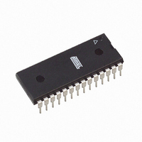
ATMEGA8L-8PU Atmel, ATMEGA8L-8PU Datasheet - Page 207

ATMEGA8L-8PU
Manufacturer Part Number
ATMEGA8L-8PU
Description
IC AVR MCU 8K 8MHZ 3V 28DIP
Manufacturer
Atmel
Series
AVR® ATmegar
Datasheets
1.ATMEGA8L-8MU.pdf
(25 pages)
2.ATMEGA8L-8MU.pdf
(302 pages)
3.ATMEGA8-16PU.pdf
(305 pages)
Specifications of ATMEGA8L-8PU
Core Processor
AVR
Core Size
8-Bit
Speed
8MHz
Connectivity
I²C, SPI, UART/USART
Peripherals
Brown-out Detect/Reset, POR, PWM, WDT
Number Of I /o
23
Program Memory Size
8KB (4K x 16)
Program Memory Type
FLASH
Eeprom Size
512 x 8
Ram Size
1K x 8
Voltage - Supply (vcc/vdd)
2.7 V ~ 5.5 V
Data Converters
A/D 6x10b
Oscillator Type
Internal
Operating Temperature
-40°C ~ 85°C
Package / Case
28-DIP (0.300", 7.62mm)
Cpu Family
ATmega
Device Core
AVR
Device Core Size
8b
Frequency (max)
8MHz
Interface Type
SPI/TWI/USART
Total Internal Ram Size
1KB
# I/os (max)
23
Number Of Timers - General Purpose
3
Operating Supply Voltage (typ)
3.3/5V
Operating Supply Voltage (max)
5.5V
Operating Supply Voltage (min)
2.7V
On-chip Adc
6-chx10-bit
Instruction Set Architecture
RISC
Operating Temp Range
-40C to 85C
Operating Temperature Classification
Industrial
Mounting
Through Hole
Pin Count
28
Package Type
PDIP
Processor Series
ATMEGA8x
Core
AVR8
Data Bus Width
8 bit
Data Ram Size
1 KB
Maximum Clock Frequency
8 MHz
Number Of Programmable I/os
23
Number Of Timers
3
Operating Supply Voltage
2.7 V to 5.5 V
Maximum Operating Temperature
+ 85 C
Mounting Style
Through Hole
3rd Party Development Tools
EWAVR, EWAVR-BL
Minimum Operating Temperature
- 40 C
Controller Family/series
AVR MEGA
No. Of I/o's
23
Eeprom Memory Size
512Byte
Ram Memory Size
1KB
Cpu Speed
8MHz
Rohs Compliant
Yes
For Use With
ATSTK600-TQFP32 - STK600 SOCKET/ADAPTER 32-TQFPATSTK600-DIP40 - STK600 SOCKET/ADAPTER 40-PDIP770-1007 - ISP 4PORT ATMEL AVR MCU SPI/JTAGATAVRISP2 - PROGRAMMER AVR IN SYSTEMATSTK500 - PROGRAMMER AVR STARTER KIT
Lead Free Status / RoHS Status
Lead free / RoHS Compliant
Available stocks
Company
Part Number
Manufacturer
Quantity
Price
Company:
Part Number:
ATMEGA8L-8PU
Manufacturer:
BROADCOM
Quantity:
101
Company:
Part Number:
ATMEGA8L-8PU
Manufacturer:
ATMEL
Quantity:
33 600
Part Number:
ATMEGA8L-8PU
Manufacturer:
ATMEL/爱特梅尔
Quantity:
20 000
Company:
Part Number:
ATMEGA8L-8PU-QS096
Manufacturer:
ATMEL
Quantity:
56
Addressing the
Flash During Self-
Programming
2486Z–AVR–02/11
• Bit 2 – PGWRT: Page Write
If this bit is written to one at the same time as SPMEN, the next SPM instruction within four clock
cycles executes page write, with the data stored in the temporary buffer. The page address is
taken from the high part of the Z-pointer. The data in R1 and R0 are ignored. The PGWRT bit
will auto-clear upon completion of a page write, or if no SPM instruction is executed within four
clock cycles. The CPU is halted during the entire page write operation if the NRWW section is
addressed.
• Bit 1 – PGERS: Page Erase
If this bit is written to one at the same time as SPMEN, the next SPM instruction within four clock
cycles executes page erase. The page address is taken from the high part of the Z-pointer. The
data in R1 and R0 are ignored. The PGERS bit will auto-clear upon completion of a page erase,
or if no SPM instruction is executed within four clock cycles. The CPU is halted during the entire
page write operation if the NRWW section is addressed.
• Bit 0 – SPMEN: Store Program Memory Enable
This bit enables the SPM instruction for the next four clock cycles. If written to one together with
either RWWSRE, BLBSET, PGWRT’ or PGERS, the following SPM instruction will have a spe-
cial meaning, see description above. If only SPMEN is written, the following SPM instruction will
store the value in R1:R0 in the temporary page buffer addressed by the Z-pointer. The LSB of
the Z-pointer is ignored. The SPMEN bit will auto-clear upon completion of an SPM instruction,
or if no SPM instruction is executed within four clock cycles. During page erase and page write,
the SPMEN bit remains high until the operation is completed.
Writing any other combination than “10001”, “01001”, “00101”, “00011” or “00001” in the lower
five bits will have no effect.
The Z-pointer is used to address the SPM commands.
Since the Flash is organized in pages (see
treated as having two different sections. One section, consisting of the least significant bits, is
addressing the words within a page, while the most significant bits are addressing the pages.
This is shown in
are addressed independently. Therefore it is of major importance that the Boot Loader software
addresses the same page in both the page erase and page write operation. Once a program-
ming operation is initiated, the address is latched and the Z-pointer can be used for other
operations.
The only SPM operation that does not use the Z-pointer is Setting the Boot Loader Lock Bits.
The content of the Z-pointer is ignored and will have no effect on the operation. The LPM
instruction does also use the Z-pointer to store the address. Since this instruction addresses the
Flash byte by byte, also the LSB (bit Z0) of the Z-pointer is used.
Bit
ZH (R31)
ZL (R30)
Z15
15
Z7
7
Figure 103 on page
Z14
Z6
14
6
Z13
13
Z5
5
208. Note that the page erase and page write operations
Z12
12
Z4
4
Table 89 on page
Z11
11
Z3
3
Z10
10
Z2
2
218), the Program Counter can be
Z9
Z1
9
1
ATmega8(L)
Z8
Z0
8
0
207


