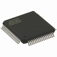
AT32UC3B0256-A2UR Atmel, AT32UC3B0256-A2UR Datasheet - Page 253

AT32UC3B0256-A2UR
Manufacturer Part Number
AT32UC3B0256-A2UR
Description
MCU AVR32 256K FLASH 64-TQFP
Manufacturer
Atmel
Series
AVR®32 UC3r
Datasheet
1.AT32UC3B1512-Z1UT.pdf
(692 pages)
Specifications of AT32UC3B0256-A2UR
Package / Case
64-TQFP, 64-VQFP
Voltage - Supply (vcc/vdd)
1.65 V ~ 1.95 V
Operating Temperature
-40°C ~ 85°C
Speed
60MHz
Number Of I /o
44
Core Processor
AVR
Program Memory Type
FLASH
Ram Size
32K x 8
Program Memory Size
256KB (256K x 8)
Data Converters
A/D 8x10b
Oscillator Type
Internal
Peripherals
Brown-out Detect/Reset, DMA, POR, PWM, WDT
Connectivity
I²C, IrDA, SPI, SSC, UART/USART, USB
Core Size
32-Bit
Package
64TQFP
Device Core
AVR32
Family Name
AT32
Maximum Speed
60 MHz
Operating Supply Voltage
1.8|3.3 V
Data Bus Width
32 Bit
Number Of Programmable I/os
44
Interface Type
I2S/SPI/TWI/USART/USB
On-chip Adc
8-chx10-bit
Number Of Timers
3
Lead Free Status / RoHS Status
Lead free / RoHS Compliant
Eeprom Size
-
Available stocks
Company
Part Number
Manufacturer
Quantity
Price
- Current page: 253 of 692
- Download datasheet (11Mb)
• SVACC: Slave Access (automatically set / reset)
• SVREAD: Slave Read (automatically set / reset)
• TXRDY: Transmit Holding Register Ready (automatically set / reset)
• RXRDY: Receive Holding Register Ready (automatically set / reset)
• TXCOMP: Transmission Completed (automatically set / reset)
32059K–03/2011
1 = A General Call has been detected. After the detection of General Call, the programmer decoded the commands that follow
and the programming sequence.
GACC behavior can be seen in
This bit is only used in Slave mode.
0 = TWI is not addressed. SVACC is automatically cleared after a NACK or a STOP condition is detected.
1 = Indicates that the address decoding sequence has matched (A Master has sent SADR). SVACC remains high until a NACK
or a STOP condition is detected.
SVACC behavior can be seen in
19-30 on page
This bit is only used in Slave mode. When SVACC is low (no Slave access has been detected) SVREAD is irrelevant.
0 = Indicates that a write access is performed by a Master.
1 = Indicates that a read access is performed by a Master.
SVREAD behavior can be seen in
19-30 on page
TXRDY used in Master mode:
0 = The transmit holding register has not been transferred into shift register. Set to 0 when writing into THR register.
1 = As soon as a data byte is transferred from THR to internal shifter or if a NACK error is detected, TXRDY is set at the same
time as TXCOMP and NACK. TXRDY is also set when MSEN is set (enable TWI).
TXRDY behavior in Master mode can be seen in
TXRDY used in Slave mode:
0 = As soon as data is written in the THR, until this data has been transmitted and acknowledged (ACK or NACK).
1 = It indicates that the THR is empty and that data has been transmitted and acknowledged.
If TXRDY is high and if a NACK has been detected, the transmission will be stopped. Thus when TRDY = NACK = 1, the
programmer must not fill THR to avoid losing it.
TXRDY behavior in Slave mode can be seen in
and
0 = No character has been received since the last RHR read operation.
1 = A byte has been received in the RHR since the last read.
RXRDY behavior in Master mode can be seen in
RXRDY behavior in Slave mode can be seen in
243
TXCOMP used in Master mode:
0 = During the length of the current frame.
1 = When both holding and shifter registers are empty and STOP condition has been sent.
TXCOMP behavior in Master mode can be seen in
TXCOMP used in Slave mode:
0 = As soon as a Start is detected.
1 = After a Stop or a Repeated Start + an address different from SADR is detected.
TXCOMP behavior in Slave mode can be seen in
243
Figure 19-30 on page
and
and
Figure 19-30 on page
Figure 19-30 on page
243.
243.
243.
243.
243.
Figure 19-26 on page
Figure 19-24 on page
Figure 19-24 on page
Figure 19-24 on page
Figure 19-25 on page
Figure 19-8 on page
Figure 19-10 on page
Figure 19-27 on page
Figure 19-8 on page 223
240.
239,
239,
Figure 19-25 on page
Figure 19-25 on page
239,
223.
239,
224.
241,
Figure 19-27 on page
Figure 19-28 on page
and in
Figure 19-28 on page
239,
Figure 19-10 on page
239,
Figure 19-29 on page 243
Figure 19-29 on page 243
241,
242,
242,
Figure 19-29 on page 243
Figure 19-29 on page
AT32UC3B
Figure 19-29 on page
224.
and
and
Figure
Figure
253
Related parts for AT32UC3B0256-A2UR
Image
Part Number
Description
Manufacturer
Datasheet
Request
R

Part Number:
Description:
DEV KIT FOR AVR/AVR32
Manufacturer:
Atmel
Datasheet:

Part Number:
Description:
INTERVAL AND WIPE/WASH WIPER CONTROL IC WITH DELAY
Manufacturer:
ATMEL Corporation
Datasheet:

Part Number:
Description:
Low-Voltage Voice-Switched IC for Hands-Free Operation
Manufacturer:
ATMEL Corporation
Datasheet:

Part Number:
Description:
MONOLITHIC INTEGRATED FEATUREPHONE CIRCUIT
Manufacturer:
ATMEL Corporation
Datasheet:

Part Number:
Description:
AM-FM Receiver IC U4255BM-M
Manufacturer:
ATMEL Corporation
Datasheet:

Part Number:
Description:
Monolithic Integrated Feature Phone Circuit
Manufacturer:
ATMEL Corporation
Datasheet:

Part Number:
Description:
Multistandard Video-IF and Quasi Parallel Sound Processing
Manufacturer:
ATMEL Corporation
Datasheet:

Part Number:
Description:
High-performance EE PLD
Manufacturer:
ATMEL Corporation
Datasheet:

Part Number:
Description:
8-bit Flash Microcontroller
Manufacturer:
ATMEL Corporation
Datasheet:

Part Number:
Description:
2-Wire Serial EEPROM
Manufacturer:
ATMEL Corporation
Datasheet:


