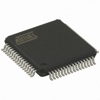
AT32UC3B0256-A2UR Atmel, AT32UC3B0256-A2UR Datasheet - Page 646

AT32UC3B0256-A2UR
Manufacturer Part Number
AT32UC3B0256-A2UR
Description
MCU AVR32 256K FLASH 64-TQFP
Manufacturer
Atmel
Series
AVR®32 UC3r
Datasheet
1.AT32UC3B1512-Z1UT.pdf
(692 pages)
Specifications of AT32UC3B0256-A2UR
Package / Case
64-TQFP, 64-VQFP
Voltage - Supply (vcc/vdd)
1.65 V ~ 1.95 V
Operating Temperature
-40°C ~ 85°C
Speed
60MHz
Number Of I /o
44
Core Processor
AVR
Program Memory Type
FLASH
Ram Size
32K x 8
Program Memory Size
256KB (256K x 8)
Data Converters
A/D 8x10b
Oscillator Type
Internal
Peripherals
Brown-out Detect/Reset, DMA, POR, PWM, WDT
Connectivity
I²C, IrDA, SPI, SSC, UART/USART, USB
Core Size
32-Bit
Package
64TQFP
Device Core
AVR32
Family Name
AT32
Maximum Speed
60 MHz
Operating Supply Voltage
1.8|3.3 V
Data Bus Width
32 Bit
Number Of Programmable I/os
44
Interface Type
I2S/SPI/TWI/USART/USB
On-chip Adc
8-chx10-bit
Number Of Timers
3
Lead Free Status / RoHS Status
Lead free / RoHS Compliant
Eeprom Size
-
Available stocks
Company
Part Number
Manufacturer
Quantity
Price
- Current page: 646 of 692
- Download datasheet (11Mb)
32059K–03/2011
- SSC
4. Increased Power Consunption in VDDIO in sleep modes
1. Additional delay on TD output
2. TF output is not correct
3. Frame Synchro and Frame Synchro Data are delayed by one clock cycle
will not be turned off. This will result in a significantly higher power consumption during the
sleep mode.
Fix/Workaround
Before going to sleep modes where the system RC oscillator is stopped, make sure that the
factor between the CPU/HSB and PBx frequencies is less than or equal to 4.
If the OSC0 is enabled in crystal mode when entering a sleep mode where the OSC0 is dis-
abled, this will lead to an increased power consumption in VDDIO.
Fix/Workaround
Disable the OSC0 through the Power Manager (PM) before going to any sleep mode where
the OSC0 is disabled, or pull down or up XIN0 and XOUT0 with 1Mohm resistor.
A delay from 2 to 3 system clock cycles is added to TD output when:
TCMR.START = Receive Start,
TCMR.STTDLY = more than ZERO,
RCMR.START = Start on falling edge / Start on Rising edge / Start on any edge,
RFMR.FSOS = None (input).
Fix/Workaround
None.
TF output is not correct (at least emitted one serial clock cycle later than expected) when:
TFMR.FSOS = Driven Low during data transfer/ Driven High during data transfer
TCMR.START = Receive start
RFMR.FSOS = None (Input)
RCMR.START = any on RF (edge/level)
Fix/Workaround
None.
The frame synchro and the frame synchro data are delayed from 1 SSC_CLOCK when:
- Clock is CKDIV
- The START is selected on either a frame synchro edge or a level
- Frame synchro data is enabled
- Transmit clock is gated on output (through CKO field)
Fix/Workaround
Transmit or receive CLOCK must not be gated (by the mean of CKO field) when START
condition is performed on a generated frame synchro.
AT32UC3B
646
Related parts for AT32UC3B0256-A2UR
Image
Part Number
Description
Manufacturer
Datasheet
Request
R

Part Number:
Description:
DEV KIT FOR AVR/AVR32
Manufacturer:
Atmel
Datasheet:

Part Number:
Description:
INTERVAL AND WIPE/WASH WIPER CONTROL IC WITH DELAY
Manufacturer:
ATMEL Corporation
Datasheet:

Part Number:
Description:
Low-Voltage Voice-Switched IC for Hands-Free Operation
Manufacturer:
ATMEL Corporation
Datasheet:

Part Number:
Description:
MONOLITHIC INTEGRATED FEATUREPHONE CIRCUIT
Manufacturer:
ATMEL Corporation
Datasheet:

Part Number:
Description:
AM-FM Receiver IC U4255BM-M
Manufacturer:
ATMEL Corporation
Datasheet:

Part Number:
Description:
Monolithic Integrated Feature Phone Circuit
Manufacturer:
ATMEL Corporation
Datasheet:

Part Number:
Description:
Multistandard Video-IF and Quasi Parallel Sound Processing
Manufacturer:
ATMEL Corporation
Datasheet:

Part Number:
Description:
High-performance EE PLD
Manufacturer:
ATMEL Corporation
Datasheet:

Part Number:
Description:
8-bit Flash Microcontroller
Manufacturer:
ATMEL Corporation
Datasheet:

Part Number:
Description:
2-Wire Serial EEPROM
Manufacturer:
ATMEL Corporation
Datasheet:


