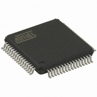
AT32UC3B0256-A2UR Atmel, AT32UC3B0256-A2UR Datasheet - Page 604

AT32UC3B0256-A2UR
Manufacturer Part Number
AT32UC3B0256-A2UR
Description
MCU AVR32 256K FLASH 64-TQFP
Manufacturer
Atmel
Series
AVR®32 UC3r
Datasheet
1.AT32UC3B1512-Z1UT.pdf
(692 pages)
Specifications of AT32UC3B0256-A2UR
Package / Case
64-TQFP, 64-VQFP
Voltage - Supply (vcc/vdd)
1.65 V ~ 1.95 V
Operating Temperature
-40°C ~ 85°C
Speed
60MHz
Number Of I /o
44
Core Processor
AVR
Program Memory Type
FLASH
Ram Size
32K x 8
Program Memory Size
256KB (256K x 8)
Data Converters
A/D 8x10b
Oscillator Type
Internal
Peripherals
Brown-out Detect/Reset, DMA, POR, PWM, WDT
Connectivity
I²C, IrDA, SPI, SSC, UART/USART, USB
Core Size
32-Bit
Package
64TQFP
Device Core
AVR32
Family Name
AT32
Maximum Speed
60 MHz
Operating Supply Voltage
1.8|3.3 V
Data Bus Width
32 Bit
Number Of Programmable I/os
44
Interface Type
I2S/SPI/TWI/USART/USB
On-chip Adc
8-chx10-bit
Number Of Timers
3
Lead Free Status / RoHS Status
Lead free / RoHS Compliant
Eeprom Size
-
Available stocks
Company
Part Number
Manufacturer
Quantity
Price
- Current page: 604 of 692
- Download datasheet (11Mb)
27.5.2.4
27.5.2.5
32059K–03/2011
INTEST
CLAMP
This instruction selects the boundary-scan chain as Data Register for testing internal logic in the
device. The logic inputs are determined by the boundary-scan chain, and the logic outputs are
captured by the boundary-scan chain. The device output pins are driven from the boundary-scan
chain.
Starting in Run-Test/Idle, the INTEST instruction is accessed the following way:
Table 27-13. INTEST Details
This instruction selects the Bypass register as Data Register. The device output pins are driven
from the boundary-scan chain.
Starting in Run-Test/Idle, the CLAMP instruction is accessed the following way:
Instructions
IR input value
IR output value
DR Size
DR input value
DR output value
1. Select the IR Scan path.
2. In Capture-IR: The IR output value is latched into the shift register.
3. In Shift-IR: The instruction register is shifted by the TCK input.
4. In Update-IR: The data from the boundary-scan chain is applied to the internal logic
5. Return to Run-Test/Idle.
6. Select the DR Scan path.
7. In Capture-DR: The data on the internal logic is sampled into the boundary-scan chain.
8. In Shift-DR: The boundary-scan chain is shifted by the TCK input.
9. In Update-DR: The data from the boundary-scan chain is applied to internal logic
10. Return to Run-Test/Idle.
1. Select the IR Scan path.
2. In Capture-IR: The IR output value is latched into the shift register.
3. In Shift-IR: The instruction register is shifted by the TCK input.
4. In Update-IR: The data from the boundary-scan chain is applied to the output pins.
5. Return to Run-Test/Idle.
6. Select the DR Scan path.
7. In Capture-DR: A logic ‘0’ is loaded into the Bypass Register.
8. In Shift-DR: Data is scanned from TDI to TDO through the Bypass register.
inputs.
inputs.
Details
00100 (0x04)
p0001
Depending on boundary-scan chain, see BSDL-file.
Depending on boundary-scan chain, see BSDL-file.
Depending on boundary-scan chain, see BSDL-file.
AT32UC3B
604
Related parts for AT32UC3B0256-A2UR
Image
Part Number
Description
Manufacturer
Datasheet
Request
R

Part Number:
Description:
DEV KIT FOR AVR/AVR32
Manufacturer:
Atmel
Datasheet:

Part Number:
Description:
INTERVAL AND WIPE/WASH WIPER CONTROL IC WITH DELAY
Manufacturer:
ATMEL Corporation
Datasheet:

Part Number:
Description:
Low-Voltage Voice-Switched IC for Hands-Free Operation
Manufacturer:
ATMEL Corporation
Datasheet:

Part Number:
Description:
MONOLITHIC INTEGRATED FEATUREPHONE CIRCUIT
Manufacturer:
ATMEL Corporation
Datasheet:

Part Number:
Description:
AM-FM Receiver IC U4255BM-M
Manufacturer:
ATMEL Corporation
Datasheet:

Part Number:
Description:
Monolithic Integrated Feature Phone Circuit
Manufacturer:
ATMEL Corporation
Datasheet:

Part Number:
Description:
Multistandard Video-IF and Quasi Parallel Sound Processing
Manufacturer:
ATMEL Corporation
Datasheet:

Part Number:
Description:
High-performance EE PLD
Manufacturer:
ATMEL Corporation
Datasheet:

Part Number:
Description:
8-bit Flash Microcontroller
Manufacturer:
ATMEL Corporation
Datasheet:

Part Number:
Description:
2-Wire Serial EEPROM
Manufacturer:
ATMEL Corporation
Datasheet:


