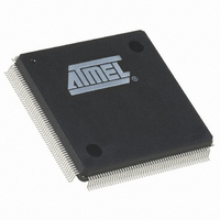
AT91SAM9260B-QU Atmel, AT91SAM9260B-QU Datasheet - Page 642

AT91SAM9260B-QU
Manufacturer Part Number
AT91SAM9260B-QU
Description
IC ARM9 MCU 208-PQFP
Manufacturer
Atmel
Series
AT91SAMr
Specifications of AT91SAM9260B-QU
Core Processor
ARM9
Core Size
16/32-Bit
Speed
180MHz
Connectivity
EBI/EMI, Ethernet, I²C, MMC, SPI, SSC, UART/USART, USB
Peripherals
POR, WDT
Number Of I /o
96
Program Memory Size
32KB (32K x 8)
Program Memory Type
ROM
Ram Size
24K x 8
Voltage - Supply (vcc/vdd)
1.65 V ~ 1.95 V
Data Converters
A/D 4x10b
Oscillator Type
Internal
Operating Temperature
-40°C ~ 85°C
Package / Case
208-MQFP, 208-PQFP
Package
208PQFP
Device Core
ARM926EJ-S
Family Name
91S
Maximum Speed
180 MHz
Operating Supply Voltage
1.8|3.3 V
Data Bus Width
32 Bit
Number Of Programmable I/os
96
Interface Type
EBI/Ethernet/SPI/TWI/UART/USART/USB
On-chip Adc
4-chx10-bit
Number Of Timers
6
Processor Series
AT91SAMx
Core
ARM926EJ-S
Data Ram Size
8 KB
Maximum Clock Frequency
180 MHz
Maximum Operating Temperature
+ 85 C
Mounting Style
SMD/SMT
3rd Party Development Tools
JTRACE-ARM-2M, MDK-ARM, RL-ARM, ULINK2
Development Tools By Supplier
AT91SAM-ICE, AT91-ISP, AT91SAM9260-EK
Minimum Operating Temperature
- 40 C
Cpu Family
AT91
Device Core Size
32b
Frequency (max)
180MHz
Total Internal Ram Size
8KB
# I/os (max)
96
Number Of Timers - General Purpose
6
Operating Supply Voltage (typ)
1.8/3.3V
Operating Supply Voltage (max)
1.95/3.6V
Operating Supply Voltage (min)
1.65/3V
Instruction Set Architecture
RISC
Operating Temp Range
-40C to 85C
Operating Temperature Classification
Industrial
Mounting
Surface Mount
Pin Count
208
Package Type
PQFP
For Use With
AT91SAM9260-EK - KIT EVAL FOR AT91SAM9260AT91SAM-ICE - EMULATOR FOR AT91 ARM7/ARM9
Lead Free Status / RoHS Status
Lead free / RoHS Compliant
Eeprom Size
-
Lead Free Status / Rohs Status
Lead free / RoHS Compliant
Available stocks
Company
Part Number
Manufacturer
Quantity
Price
Company:
Part Number:
AT91SAM9260B-QU
Manufacturer:
ATMEL
Quantity:
2 000
Company:
Part Number:
AT91SAM9260B-QU
Manufacturer:
ATMEL
Quantity:
9
Part Number:
AT91SAM9260B-QU
Manufacturer:
AT
Quantity:
20 000
- Current page: 642 of 798
- Download datasheet (12Mb)
Figure 36-10. Bank Swapping in Data OUT Transfers for Ping-pong Endpoints
642
AT91SAM9260
1 st Data Payload
2 nd Data Payload
3 rd Data Payload
Microcontroller
Write and Read at the Same Time
load sent by the host, while the current data payload is received by the USB device. Thus two
banks of memory are used. While one is available for the microcontroller, the other one is locked
by the USB device.
When using a ping-pong endpoint, the following procedures are required to perform Data OUT
transactions:
1. The host generates a Data OUT packet.
2. This packet is received by the USB device endpoint. It is written in the endpoint’s FIFO
3. The USB device sends an ACK PID packet to the host. The host can immediately send
4. The microcontroller is notified that the USB device has received a data payload, polling
5. The number of bytes available in the FIFO is made available by reading RXBYTECNT
6. The microcontroller transfers out data received from the endpoint’s memory to the
7. The microcontroller notifies the USB peripheral device that it has finished the transfer
8. A third Data OUT packet can be accepted by the USB peripheral device and copied in
9. If a second Data OUT packet has been received, the microcontroller is notified by the
10. The microcontroller transfers out data received from the endpoint’s memory to the
Bank 0.
a second Data OUT packet. It is accepted by the device and copied to FIFO Bank 1.
RX_DATA_BK0 in the endpoint’s UDP_CSRx register. An interrupt is pending for this
endpoint while RX_DATA_BK0 is set.
in the endpoint’s UDP_CSRx register.
microcontroller’s memory. Data received is made available by reading the endpoint’s
UDP_FDRx register.
by clearing RX_DATA_BK0 in the endpoint’s UDP_CSRx register.
the FIFO Bank 0.
flag RX_DATA_BK1 set in the endpoint’s UDP_CSRx register. An interrupt is pending
for this endpoint while RX_DATA_BK1 is set.
microcontroller’s memory. Data received is available by reading the endpoint’s
UDP_FDRx register.
Bank 0
Endpoint 1
Bank 1
Endpoint 1
Bank 0
Endpoint 1
Write
USB Device
Bank 0
Endpoint 1
Bank 1
Endpoint 1
Bank 0
Endpoint 1
Read
USB Bus
2 nd Data Payload
3 rd Data Payload
1 st Data Payload
Data IN Packet
Data IN Packet
Data IN Packet
6221I–ATARM–17-Jul-09
Related parts for AT91SAM9260B-QU
Image
Part Number
Description
Manufacturer
Datasheet
Request
R

Part Number:
Description:
MCU, MPU & DSP Development Tools KICKSTART KIT FOR AT91SAM9 PLUS
Manufacturer:
IAR Systems

Part Number:
Description:
DEV KIT FOR AVR/AVR32
Manufacturer:
Atmel
Datasheet:

Part Number:
Description:
INTERVAL AND WIPE/WASH WIPER CONTROL IC WITH DELAY
Manufacturer:
ATMEL Corporation
Datasheet:

Part Number:
Description:
Low-Voltage Voice-Switched IC for Hands-Free Operation
Manufacturer:
ATMEL Corporation
Datasheet:

Part Number:
Description:
MONOLITHIC INTEGRATED FEATUREPHONE CIRCUIT
Manufacturer:
ATMEL Corporation
Datasheet:

Part Number:
Description:
AM-FM Receiver IC U4255BM-M
Manufacturer:
ATMEL Corporation
Datasheet:

Part Number:
Description:
Monolithic Integrated Feature Phone Circuit
Manufacturer:
ATMEL Corporation
Datasheet:

Part Number:
Description:
Multistandard Video-IF and Quasi Parallel Sound Processing
Manufacturer:
ATMEL Corporation
Datasheet:

Part Number:
Description:
High-performance EE PLD
Manufacturer:
ATMEL Corporation
Datasheet:

Part Number:
Description:
8-bit Flash Microcontroller
Manufacturer:
ATMEL Corporation
Datasheet:

Part Number:
Description:
2-Wire Serial EEPROM
Manufacturer:
ATMEL Corporation
Datasheet:


