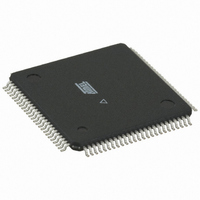
ATMEGA2560V-8AU Atmel, ATMEGA2560V-8AU Datasheet - Page 153

ATMEGA2560V-8AU
Manufacturer Part Number
ATMEGA2560V-8AU
Description
IC AVR MCU 256K 8MHZ 100TQFP
Manufacturer
Atmel
Series
AVR® ATmegar
Datasheets
1.ATMEGA640V-8CU.pdf
(38 pages)
2.ATMEGA640V-8CU.pdf
(444 pages)
3.ATMEGA2560V-8AU.pdf
(37 pages)
Specifications of ATMEGA2560V-8AU
Core Processor
AVR
Core Size
8-Bit
Speed
8MHz
Connectivity
EBI/EMI, I²C, SPI, UART/USART
Peripherals
Brown-out Detect/Reset, POR, PWM, WDT
Number Of I /o
86
Program Memory Size
256KB (128K x 16)
Program Memory Type
FLASH
Eeprom Size
4K x 8
Ram Size
8K x 8
Voltage - Supply (vcc/vdd)
1.8 V ~ 5.5 V
Data Converters
A/D 16x10b
Oscillator Type
Internal
Operating Temperature
-40°C ~ 85°C
Package / Case
100-TQFP, 100-VQFP
Processor Series
ATMEGA256x
Core
AVR8
Data Bus Width
8 bit
Data Ram Size
8 KB
Interface Type
2-Wire, SPI, USART
Maximum Clock Frequency
8 MHz
Number Of Programmable I/os
86
Number Of Timers
6
Operating Supply Voltage
1.8 V to 5.5 V
Maximum Operating Temperature
+ 85 C
Mounting Style
SMD/SMT
3rd Party Development Tools
EWAVR, EWAVR-BL
Minimum Operating Temperature
- 40 C
On-chip Adc
10 bit, 16 Channel
A/d Inputs
16-Channel, 10-Bit
Cpu Speed
8 MIPS
Eeprom Memory
4K Bytes
Input Output
86
Interface
2-Wire/SPI/USART
Memory Type
Flash
Number Of Bits
8
Package Type
100-pin TQFP
Programmable Memory
256K Bytes
Timers
2-8-bit, 4-16-bit
Voltage, Range
1.8-5.5 V
Package
100TQFP
Device Core
AVR
Family Name
ATmega
Maximum Speed
8 MHz
For Use With
ATSTK600-TQFP100 - STK600 SOCKET/ADAPTER 100-TQFP770-1007 - ISP 4PORT ATMEL AVR MCU SPI/JTAG770-1005 - ISP 4PORT FOR ATMEL AVR MCU JTAG770-1004 - ISP 4PORT FOR ATMEL AVR MCU SPIATAVRISP2 - PROGRAMMER AVR IN SYSTEMATSTK503 - STARTER KIT AVR EXP MODULE 100PATJTAGICE2 - AVR ON-CHIP D-BUG SYSTEM
Lead Free Status / RoHS Status
Lead free / RoHS Compliant
Available stocks
Company
Part Number
Manufacturer
Quantity
Price
Company:
Part Number:
ATMEGA2560V-8AU
Manufacturer:
Atmel
Quantity:
900
Part Number:
ATMEGA2560V-8AU
Manufacturer:
ATMEL/爱特梅尔
Quantity:
20 000
- Current page: 153 of 444
- Download datasheet (10Mb)
2549M–AVR–09/10
Figure 16-8. Phase Correct PWM Mode, Timing Diagram
The Timer/Counter Overflow Flag (TOVn) is set each time the counter reaches BOTTOM. When
either OCRnA or ICRn is used for defining the TOP value, the OCnA or ICFn Flag is set accord-
ingly at the same timer clock cycle as the OCRnx Registers are updated with the double buffer
value (at TOP). The Interrupt Flags can be used to generate an interrupt each time the counter
reaches the TOP or BOTTOM value.
When changing the TOP value the program must ensure that the new TOP value is higher or
equal to the value of all of the Compare Registers. If the TOP value is lower than any of the
Compare Registers, a compare match will never occur between the TCNTn and the OCRnx.
Note that when using fixed TOP values, the unused bits are masked to zero when any of the
OCRnx Registers are written. As the third period shown in
TOP actively while the Timer/Counter is running in the phase correct mode can result in an
unsymmetrical output. The reason for this can be found in the time of update of the OCRnx Reg-
ister. Since the OCRnx update occurs at TOP, the PWM period starts and ends at TOP. This
implies that the length of the falling slope is determined by the previous TOP value, while the
length of the rising slope is determined by the new TOP value. When these two values differ the
two slopes of the period will differ in length. The difference in length gives the unsymmetrical
result on the output.
It is recommended to use the phase and frequency correct mode instead of the phase correct
mode when changing the TOP value while the Timer/Counter is running. When using a static
TOP value there are practically no differences between the two modes of operation.
In phase correct PWM mode, the compare units allow generation of PWM waveforms on the
OCnx pins. Setting the COMnx1:0 bits to two will produce a non-inverted PWM and an inverted
PWM output can be generated by setting the COMnx1:0 to three (see
The actual OCnx value will only be visible on the port pin if the data direction for the port pin is
set as output (DDR_OCnx). The PWM waveform is generated by setting (or clearing) the OCnx
Register at the compare match between OCRnx and TCNTn when the counter increments, and
clearing (or setting) the OCnx Register at compare match between OCRnx and TCNTn when
TCNTn
OCnx
OCnx
Period
1
ATmega640/1280/1281/2560/2561
2
3
Figure 16-8
4
Table 16-5 on page
illustrates, changing the
OCRnx/TOP Update and
OCnA Interrupt Flag Set
or ICFn Interrupt Flag Set
(Interrupt on TOP)
TOVn Interrupt Flag Set
(Interrupt on Bottom)
(COMnx1:0 = 2)
(COMnx1:0 = 3)
160).
153
Related parts for ATMEGA2560V-8AU
Image
Part Number
Description
Manufacturer
Datasheet
Request
R

Part Number:
Description:
IC AVR MCU 2.4GHZ XCEIVER 64QFN
Manufacturer:
Atmel
Datasheet:

Part Number:
Description:
Manufacturer:
Atmel
Datasheet:

Part Number:
Description:
MCU ATMEGA644/AT86RF230 40-DIP
Manufacturer:
Atmel
Datasheet:

Part Number:
Description:
BUNDLE ATMEGA644P/AT86RF230 QFN
Manufacturer:
Atmel
Datasheet:

Part Number:
Description:
BUNDLE ATMEGA644P/AT86RF230 TQFP
Manufacturer:
Atmel
Datasheet:

Part Number:
Description:
MCU ATMEGA1281/AT86RF230 64-TQFP
Manufacturer:
Atmel
Datasheet:

Part Number:
Description:
MCU ATMEGA1280/AT86RF230 100TQFP
Manufacturer:
Atmel
Datasheet:

Part Number:
Description:
BUNDLE ATMEGA1280/AT86RF100-TQFP
Manufacturer:
Atmel
Datasheet:

Part Number:
Description:
BUNDLE ATMEGA2560V/AT86RF230-ZU
Manufacturer:
Atmel
Datasheet:

Part Number:
Description:
MCU ATMEGA2561/AT86RF230 64-TQFP
Manufacturer:
Atmel
Datasheet:

Part Number:
Description:
INTERVAL AND WIPE/WASH WIPER CONTROL IC WITH DELAY
Manufacturer:
ATMEL Corporation
Datasheet:

Part Number:
Description:
Low-Voltage Voice-Switched IC for Hands-Free Operation
Manufacturer:
ATMEL Corporation
Datasheet:

Part Number:
Description:
MONOLITHIC INTEGRATED FEATUREPHONE CIRCUIT
Manufacturer:
ATMEL Corporation
Datasheet:

Part Number:
Description:
AM-FM Receiver IC U4255BM-M
Manufacturer:
ATMEL Corporation
Datasheet:


