P89V662FBC,557 NXP Semiconductors, P89V662FBC,557 Datasheet - Page 27

P89V662FBC,557
Manufacturer Part Number
P89V662FBC,557
Description
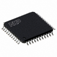
IC 80C51 MCU FLASH 32K 44-TQFP
Manufacturer
NXP Semiconductors
Series
89Vr
Datasheet
1.P89V660FBC557.pdf
(89 pages)
Specifications of P89V662FBC,557
Program Memory Type
FLASH
Program Memory Size
32KB (32K x 8)
Package / Case
44-TQFP
Core Processor
8051
Core Size
8-Bit
Speed
40MHz
Connectivity
I²C, SPI, UART/USART
Peripherals
POR, PWM, WDT
Number Of I /o
36
Ram Size
1K x 8
Voltage - Supply (vcc/vdd)
4.5 V ~ 5.5 V
Oscillator Type
Internal
Operating Temperature
-40°C ~ 85°C
Processor Series
P89V6x
Core
80C51
Data Bus Width
8 bit
Data Ram Size
1 KB
Interface Type
I2C/UART
Maximum Clock Frequency
40 MHz
Number Of Programmable I/os
36
Number Of Timers
3
Operating Supply Voltage
4.5 V to 5.5 V
Maximum Operating Temperature
+ 85 C
Mounting Style
SMD/SMT
3rd Party Development Tools
PK51, CA51, A51, ULINK2
Minimum Operating Temperature
- 40 C
Lead Free Status / RoHS Status
Lead free / RoHS Compliant
For Use With
622-1001 - USB IN-CIRCUIT PROG 80C51ISP
Eeprom Size
-
Data Converters
-
Lead Free Status / Rohs Status
Lead free / RoHS Compliant
Other names
568-2435
935280832557
P89V662FBC
935280832557
P89V662FBC
Available stocks
Company
Part Number
Manufacturer
Quantity
Price
Company:
Part Number:
P89V662FBC,557
Manufacturer:
Maxim
Quantity:
260
Company:
Part Number:
P89V662FBC,557
Manufacturer:
NXP Semiconductors
Quantity:
10 000
NXP Semiconductors
Table 16.
Table 17.
P89V660_662_664_3
Product data sheet
Bit
7,1,0
2
3
4
5
6
CR2:0
000
001
010
011
100
Symbol
CR2:0
AA
SI
STO
STA
ENS1
6-clock mode
6 MHz
47
54
63
75
12.5
I
I
2
2
C-bus control register (S1CON - address D8H) bit description
C-bus clock rates
Description
SCL clock selection. See
The Assert Acknowledge Flag. When set to 1, an acknowledge (LOW-state to SDA) will be returned
during the acknowledge clock pulse on the SCL line on the following situations:
When cleared to 0, an not acknowledge (HIGH-state to SDA) will be returned during the acknowledge
clock pulse on the SCL line on the following situations:
I
bit and EI2C (IEN1.0) bit are both set, an interrupt is requested when SI is set. Must be cleared by
software by writing 0 to this bit.
STOP Flag. STO = 1: In master mode, a STOP condition is transmitted to the I
detects the STOP condition, it will clear STO bit automatically. In slave mode, setting this bit can
recover from an error condition. In this case, no STOP condition is transmitted to the bus. The
hardware behaves as if a STOP condition has been received and it switches to ‘not addressed’ Slave
Receiver mode. The STO flag is cleared by hardware automatically.
Start Flag. STA = 1: I
the bus is free. If the bus is not free, it waits for a STOP condition (which will free the bus) and
generates a START condition after a delay of a half clock period of the internal clock generator. When
the I
a repeated START condition. STA may be set at any time, it may also be set when the I
interface is in an addressed slave mode. STA = 0: no START condition or repeated START condition
will be generated.
I
disabled.
2
2
1. The ‘own slave address’ has been received.
2. The general call address has been received while the general call bit (GC) in S1ADR is set.
3. A data byte has been received while the I
4. A data byte has been received while the I
1. A data byte has been received while the I
2. A data byte has been received while the I
C-bus Interrupt Flag. This bit is set when one of the 25 possible I
C-bus Interface Enable. When set, enables the I
Table 15.
Bit
Symbol
Reset
2
mode.
mode.
C-bus interface is already in master mode and some data is transmitted or received, it transmits
12 MHZ
94
107
125
150
25
7
CR2
x
I
2
Bit frequency at f
C-bus control register (S1CON - address D8H) bit allocation
2
C-bus enters master mode, checks the bus and generates a START condition if
6
ENS1
0
Table
Rev. 03 — 10 November 2008
12-clock mode
6 MHz
23
27
31
37
6.25
17.
osc
5
STA
0
80C51 with 512 B/1 kB/2 kB RAM, dual I
2
2
2
2
12 MHz
47
54
63
75
12.5
C-bus interface is in the Master Receiver mode.
C-bus interface is in the addressed Slave Receiver
C-bus interface is in the Master Receiver mode.
C-bus interface is in the addressed Slave Receiver
4
STO
0
2
C-bus interface. When clear, the I
3
SI
0
P89V660/662/664
f
6X
128
112
96
80
480
2
osc
C-bus states is entered. When EA
divided by
2
AA
0
2
C-bus. When the bus
1
CR1
x
© NXP B.V. 2008. All rights reserved.
2
12X
256
224
192
160
960
C-bus function is
2
C-bus
2
C-bus, SPI
0
CR0
0
27 of 89


