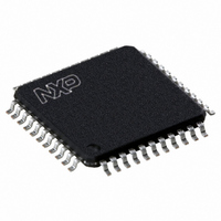
P89V662FBC,557 NXP Semiconductors, P89V662FBC,557 Datasheet - Page 55

P89V662FBC,557
Manufacturer Part Number
P89V662FBC,557
Description
IC 80C51 MCU FLASH 32K 44-TQFP
Manufacturer
NXP Semiconductors
Series
89Vr
Datasheet
1.P89V660FBC557.pdf
(89 pages)
Specifications of P89V662FBC,557
Program Memory Type
FLASH
Program Memory Size
32KB (32K x 8)
Package / Case
44-TQFP
Core Processor
8051
Core Size
8-Bit
Speed
40MHz
Connectivity
I²C, SPI, UART/USART
Peripherals
POR, PWM, WDT
Number Of I /o
36
Ram Size
1K x 8
Voltage - Supply (vcc/vdd)
4.5 V ~ 5.5 V
Oscillator Type
Internal
Operating Temperature
-40°C ~ 85°C
Processor Series
P89V6x
Core
80C51
Data Bus Width
8 bit
Data Ram Size
1 KB
Interface Type
I2C/UART
Maximum Clock Frequency
40 MHz
Number Of Programmable I/os
36
Number Of Timers
3
Operating Supply Voltage
4.5 V to 5.5 V
Maximum Operating Temperature
+ 85 C
Mounting Style
SMD/SMT
3rd Party Development Tools
PK51, CA51, A51, ULINK2
Minimum Operating Temperature
- 40 C
Lead Free Status / RoHS Status
Lead free / RoHS Compliant
For Use With
622-1001 - USB IN-CIRCUIT PROG 80C51ISP
Eeprom Size
-
Data Converters
-
Lead Free Status / Rohs Status
Lead free / RoHS Compliant
Other names
568-2435
935280832557
P89V662FBC
935280832557
P89V662FBC
Available stocks
Company
Part Number
Manufacturer
Quantity
Price
Company:
Part Number:
P89V662FBC,557
Manufacturer:
Maxim
Quantity:
260
Company:
Part Number:
P89V662FBC,557
Manufacturer:
NXP Semiconductors
Quantity:
10 000
NXP Semiconductors
P89V660_662_664_3
Product data sheet
Table 41.
Table 42.
Table 43.
Bit addressable; Reset source(s): any reset; Reset value: 0000 0000B
Table 44.
Bit
2
1
0
SPR1
0
0
1
1
Bit
7
6
5 to 0
Bit
Symbol
Fig 24. SPI transfer format with CPHA = 0
SCK (CPOL = 0)
SCK (CPOL = 1)
(for reference)
(from master)
SS (to slave)
SCK cycle #
(from slave)
SPCR - SPI control register (address D5H) bit description
SPCR - SPI control register (address D5H) clock rate selection
SPSR - SPI status register (address AAH) bit allocation
SPSR - SPI status register (address AAH) bit description
Symbol
CPHA
SPR1
SPR0
Symbol
SPIF
WCOL
-
SPIF
MOSI
MISO
7
SPR0
0
1
0
1
Rev. 03 — 10 November 2008
WCOL
6
Description
Clock Phase control bit. 1 = shift triggered on the trailing edge of the
clock; 0 = shift triggered on the leading edge of the clock.
SPI Clock Rate Select bit 1. Along with SPR0 controls the SCK rate of
the device when a master. SPR1 and SPR0 have no effect on the
slave. See
SPI Clock Rate Select bit 0. Along with SPR1 controls the SCK rate of
the device when a master. SPR1 and SPR0 have no effect on the
slave. See
Description
SPI interrupt flag. Upon completion of data transfer, this bit is set to ‘1’.
If SPIE = 1 and ES3 = 1, an interrupt is then generated. This bit is
cleared by software.
Write Collision Flag. Set if the SPI data register is written to during
data transfer. This bit is cleared by software.
Reserved for future use. Should be set to ‘0’ by user programs.
MSB
MSB
1
2
6
6
5
-
80C51 with 512 B/1 kB/2 kB RAM, dual I
Table
Table
SCK = f
6-clock mode
2
8
32
64
3
5
5
42.
42.
4
-
osc
4
4
4
divided by
5
3
3
P89V660/662/664
3
-
6
2
2
7
12-clock mode
4
16
64
128
1
1
2
-
…continued
LSB
LSB
8
© NXP B.V. 2008. All rights reserved.
1
-
002aaa529
2
C-bus, SPI
55 of 89
0
-


