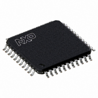
P89V662FBC,557 NXP Semiconductors, P89V662FBC,557 Datasheet - Page 41

P89V662FBC,557
Manufacturer Part Number
P89V662FBC,557
Description
IC 80C51 MCU FLASH 32K 44-TQFP
Manufacturer
NXP Semiconductors
Series
89Vr
Datasheet
1.P89V660FBC557.pdf
(89 pages)
Specifications of P89V662FBC,557
Program Memory Type
FLASH
Program Memory Size
32KB (32K x 8)
Package / Case
44-TQFP
Core Processor
8051
Core Size
8-Bit
Speed
40MHz
Connectivity
I²C, SPI, UART/USART
Peripherals
POR, PWM, WDT
Number Of I /o
36
Ram Size
1K x 8
Voltage - Supply (vcc/vdd)
4.5 V ~ 5.5 V
Oscillator Type
Internal
Operating Temperature
-40°C ~ 85°C
Processor Series
P89V6x
Core
80C51
Data Bus Width
8 bit
Data Ram Size
1 KB
Interface Type
I2C/UART
Maximum Clock Frequency
40 MHz
Number Of Programmable I/os
36
Number Of Timers
3
Operating Supply Voltage
4.5 V to 5.5 V
Maximum Operating Temperature
+ 85 C
Mounting Style
SMD/SMT
3rd Party Development Tools
PK51, CA51, A51, ULINK2
Minimum Operating Temperature
- 40 C
Lead Free Status / RoHS Status
Lead free / RoHS Compliant
For Use With
622-1001 - USB IN-CIRCUIT PROG 80C51ISP
Eeprom Size
-
Data Converters
-
Lead Free Status / Rohs Status
Lead free / RoHS Compliant
Other names
568-2435
935280832557
P89V662FBC
935280832557
P89V662FBC
Available stocks
Company
Part Number
Manufacturer
Quantity
Price
Company:
Part Number:
P89V662FBC,557
Manufacturer:
Maxim
Quantity:
260
Company:
Part Number:
P89V662FBC,557
Manufacturer:
NXP Semiconductors
Quantity:
10 000
NXP Semiconductors
P89V660_662_664_3
Product data sheet
6.5.2 Mode 1
6.5.3 Mode 2
In this mode, the Timer register is configured as a 13-bit register. As the count rolls over
from all 1s to all 0s, it sets the Timer interrupt flag TFn. The count input is enabled to the
Timer when TRn = 1 and either GATE = 0 or INTn = 1. (Setting GATE = 1 allows the Timer
to be controlled by external input INTn, to facilitate pulse width measurements). TRn is a
control bit in the Special Function Register TCON
register.
The 13-bit register consists of all 8 bits of THn and the lower 5 bits of TLn. The upper
3 bits of TLn are indeterminate and should be ignored. Setting the run flag (TRn) does not
clear the registers.
Mode 0 operation is the same for Timer 0 and Timer 1 (see
different GATE bits, one for Timer 1 (TMOD.7) and one for Timer 0 (TMOD.3).
Mode 1 is the same as Mode 0, except that all 16 bits of the timer register (THn and TLn)
are used. See
Mode 2 configures the Timer register as an 8-bit Counter (TLn) with automatic reload, as
shown in
contents of THn, which must be preset by software. The reload leaves THn unchanged.
Mode 2 operation is the same for Timer 0 and Timer 1.
Fig 14. Timer/Counter 0 or 1 in Mode 0 (13-bit counter)
Fig 15. Timer/Counter 0 or 1 in Mode 1 (16-bit counter)
INTn pin
TnGate
INTn pin
Tn pin
TnGate
osc/6
Tn pin
TRn
osc/6
TRn
Figure
Figure
16. Overflow from TLn not only sets TFn, but also reloads TLn with the
Rev. 03 — 10 November 2008
15.
C/T = 0
C/T = 1
C/T = 0
C/T = 1
80C51 with 512 B/1 kB/2 kB RAM, dual I
control
control
(Figure
(8-bits)
(5-bits)
TLn
TLn
P89V660/662/664
5). The GATE bit is in the TMOD
(8-bits)
(8-bits)
THn
THn
Figure
overflow
overflow
14). There are two
© NXP B.V. 2008. All rights reserved.
TFn
TFn
2
002aaa519
C-bus, SPI
002aaa520
interrupt
interrupt
41 of 89


