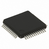
ST72F63BH6T1 STMicroelectronics, ST72F63BH6T1 Datasheet - Page 44

ST72F63BH6T1
Manufacturer Part Number
ST72F63BH6T1
Description
IC MCU 8BIT 32K FLASH 48-LQFP
Manufacturer
STMicroelectronics
Series
ST7r
Datasheet
1.ST72F63BD6U1TR.pdf
(186 pages)
Specifications of ST72F63BH6T1
Core Processor
ST7
Core Size
8-Bit
Speed
8MHz
Connectivity
I²C, SCI, USB
Peripherals
DMA, LVD, POR, PWM, WDT
Number Of I /o
27
Program Memory Size
32KB (32K x 8)
Program Memory Type
FLASH
Ram Size
1K x 8
Voltage - Supply (vcc/vdd)
4 V ~ 5.5 V
Data Converters
A/D 12x8b
Oscillator Type
External
Operating Temperature
0°C ~ 70°C
Package / Case
48-LQFP
Processor Series
ST72F6x
Core
ST7
Data Bus Width
8 bit
Data Ram Size
1 KB
Interface Type
I2C, SCI
Maximum Clock Frequency
8 MHz
Number Of Programmable I/os
27
Number Of Timers
1
Maximum Operating Temperature
+ 70 C
Mounting Style
SMD/SMT
Development Tools By Supplier
ST7MDTU3-EPB/US, ST72F63B-SK/RAIS, ST7MDTU3-EMU3, STX-RLINK
Minimum Operating Temperature
0 C
On-chip Adc
8 bit, 8 Channel / 8 bit, 12 Channel
For Use With
497-5521 - EVAL BOARD LOW SPEED USB
Lead Free Status / RoHS Status
Lead free / RoHS Compliant
Eeprom Size
-
Lead Free Status / Rohs Status
Details
Available stocks
Company
Part Number
Manufacturer
Quantity
Price
Company:
Part Number:
ST72F63BH6T1
Manufacturer:
TI
Quantity:
10
Company:
Part Number:
ST72F63BH6T1
Manufacturer:
STMicroelectronics
Quantity:
10 000
I/O ports
Note:
Note:
Caution:
44/186
1
2
Output mode
The pin is configured in output mode by setting the corresponding DDR register bit (see
Table 7).
In this mode, writing “0” or “1” to the DR register applies this digital value to the I/O pin
through the latch. Therefore, the previously saved value is restored when the DR register is
read.
The interrupt function is disabled in this mode.
Digital alternate function
When an on-chip peripheral is configured to use a pin, the alternate function is automatically
selected. This alternate function takes priority over standard I/O programming. When the
signal is coming from an on-chip peripheral, the I/O pin is automatically configured in output
mode (push-pull or open drain according to the peripheral).
When the signal is going to an on-chip peripheral, the I/O pin has to be configured in input
mode. In this case, the pin’s state is also digitally readable by addressing the DR register.
Input pull-up configuration can cause an unexpected value at the input of the alternate
peripheral input.
When the on-chip peripheral uses a pin as input and output, this pin must be configured as
an input (DDR = 0).
The alternate function must not be activated as long as the pin is configured as an input with
interrupt in order to avoid generating spurious interrupts.
Analog alternate function
When the pin is used as an ADC input the I/O must be configured as a floating input. The
analog multiplexer (controlled by the ADC registers) switches the analog voltage present on
the selected pin to the common analog rail which is connected to the ADC input.
It is recommended not to change the voltage level or loading on any port pin while
conversion is in progress. Furthermore it is recommended not to have clocking pins located
close to a selected analog pin.
Warning:
The analog input voltage level must be within the limits
stated in the absolute maximum ratings.
Doc ID 7516 Rev 8
ST7263Bxx


