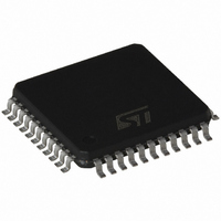
ST72F561J4T6 STMicroelectronics, ST72F561J4T6 Datasheet - Page 177

ST72F561J4T6
Manufacturer Part Number
ST72F561J4T6
Description
IC MCU 8BIT 16K FLASH 44-LQFP
Manufacturer
STMicroelectronics
Series
ST7r
Datasheet
1.ST72F561K6T6.pdf
(265 pages)
Specifications of ST72F561J4T6
Core Processor
ST7
Core Size
8-Bit
Speed
8MHz
Connectivity
CAN, LINSCI, SPI
Peripherals
LVD, POR, PWM, WDT
Number Of I /o
32
Program Memory Size
16KB (16K x 8)
Program Memory Type
FLASH
Ram Size
1K x 8
Voltage - Supply (vcc/vdd)
3.8 V ~ 5.5 V
Data Converters
A/D 16x10b
Oscillator Type
External
Operating Temperature
-40°C ~ 85°C
Package / Case
44-LQFP
Processor Series
ST72F5x
Core
ST7
Data Bus Width
8 bit
Data Ram Size
1 KB
Interface Type
CAN, SCI, SPI
Maximum Clock Frequency
8 MHz
Number Of Programmable I/os
48
Number Of Timers
3
Maximum Operating Temperature
+ 85 C
Mounting Style
SMD/SMT
Development Tools By Supplier
STX-RLINK
Minimum Operating Temperature
- 40 C
On-chip Adc
10 bit, 16 Channel
For Use With
497-8374 - BOARD DEVELOPMENT FOR ST72F561
Lead Free Status / RoHS Status
Lead free / RoHS Compliant
Eeprom Size
-
Lead Free Status / Rohs Status
Details
Available stocks
Company
Part Number
Manufacturer
Quantity
Price
Company:
Part Number:
ST72F561J4T6
Manufacturer:
COILCRAFT
Quantity:
4 000
Company:
Part Number:
ST72F561J4T6
Manufacturer:
STMicroelectronics
Quantity:
10 000
beCAN CONTROLLER (Cont’d)
FIFO Management
Starting from the empty state, the first valid mes-
sage received is stored in the FIFO which be-
comes pending_1. The hardware signals the
event setting the FMP[1:0] bits in the CRFR regis-
ter to the value 01b. The message is available in
the FIFO output mailbox. The software reads out
the mailbox content and releases it by setting the
RFOM bit in the CRFR register. The FIFO be-
comes empty again. If a new valid message has
been received in the meantime, the FIFO stays in
pending_1 state and the new message is availa-
ble in the output mailbox.
If the application does not release the mailbox, the
next valid message will be stored in the FIFO
which enters pending_2 state (FMP[1:0] = 10b).
The storage process is repeated for the next valid
message putting the FIFO into pending_3 state
(FMP[1:0] = 11b). At this point, the software must
release the output mailbox by setting the RFOM
bit, so that a mailbox is free to store the next valid
message. Otherwise the next valid message re-
ceived will cause a loss of message.
Refer also to
Overrun
Once the FIFO is in pending_3 state (that is, the
three mailboxes are full) the next valid message
reception will lead to an overrun and a message
will be lost. The hardware signals the overrun con-
dition by setting the FOVR bit in the CRFR regis-
ter. Which message is lost depends on the config-
uration of the FIFO:
– If the FIFO lock function is disabled (RFLM bit in
– If the FIFO lock function is enabled (RFLM bit in
Reception Related Interrupts
On the storage of the first message in the FIFO -
FMP[1:0] bits change from 00b to 01b - an inter-
rupt is generated if the FMPIE bit in the CIER reg-
ister is set.
When the FIFO becomes full (that is, a third mes-
sage is stored) the FULL bit in the CRFR register
is set and an interrupt is generated if the FFIE bit in
the CIER register is set.
the CMCR register cleared) the last message
stored in the FIFO will be overwritten by the new
incoming message. In this case the latest mes-
sages will be always available to the application.
the CMCR register set) the most recent message
will be discarded and the software will have the
three oldest messages in the FIFO available.
Section 0.1.4.4 Message
Storage.
On overrun condition, the FOVR bit is set and an
interrupt is generated if the FOVIE bit in the CIER
register is set.
10.9.4.3 Identifier Filtering
In the CAN protocol the identifier of a message is
not associated with the address of a node but re-
lated to the content of the message. Consequently
a transmitter broadcasts its message to all receiv-
ers. On message reception a receiver node de-
cides - depending on the identifier value - whether
the software needs the message or not. If the mes-
sage is needed, it is copied into the RAM. If not,
the message must be discarded without interven-
tion by the software.
To fulfil this requirement, the beCAN Controller
provides six configurable and scalable filter banks
(0-5) in order to receive only the messages the
software needs. This hardware filtering saves
CPU resources which would be otherwise needed
to perform filtering by software. Each filter bank
consists of eight 8-bit registers, CFxR[0:7].
Scalable Width
To optimize and adapt the filters to the application
needs, each filter bank can be scaled independ-
ently. Depending on the filter scale a filter bank
provides:
– One 32-bit filter for the STDID[10:0], IDE, EX-
– Two 16-bit filters for the STDID[10:0], RTR and
– Four 8-bit filters for the STDID[10:3] bits. The
– One 16-bit filter and two 8-bit filters for filtering
Refer to
Register
Furthermore, the filters can be configured in mask
mode or in identifier list mode.
Mask mode
In mask mode the identifier registers are associat-
ed with mask registers specifying which bits of the
identifier are handled as “must match” or as “don’t
care”.
Identifier List mode
In identifier list mode, the mask registers are
used as identifier registers. Thus instead of defin-
ing an identifier and a mask, two identifiers are
specified, doubling the number of single identifi-
ers. All bits of the incoming identifier must match
the bits specified in the filter registers.
TID[17:0] and RTR bits.
IDE bits.
other bits are considered as “don’t care”.
the same set of bits as the 16 and 8-bit filters de-
scribed above.
Figure 9. Filter Bank Scale Configuration -
Organisation.
ST72561
177/265


