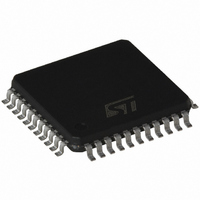
ST72F561J4T6 STMicroelectronics, ST72F561J4T6 Datasheet - Page 21

ST72F561J4T6
Manufacturer Part Number
ST72F561J4T6
Description
IC MCU 8BIT 16K FLASH 44-LQFP
Manufacturer
STMicroelectronics
Series
ST7r
Datasheet
1.ST72F561K6T6.pdf
(265 pages)
Specifications of ST72F561J4T6
Core Processor
ST7
Core Size
8-Bit
Speed
8MHz
Connectivity
CAN, LINSCI, SPI
Peripherals
LVD, POR, PWM, WDT
Number Of I /o
32
Program Memory Size
16KB (16K x 8)
Program Memory Type
FLASH
Ram Size
1K x 8
Voltage - Supply (vcc/vdd)
3.8 V ~ 5.5 V
Data Converters
A/D 16x10b
Oscillator Type
External
Operating Temperature
-40°C ~ 85°C
Package / Case
44-LQFP
Processor Series
ST72F5x
Core
ST7
Data Bus Width
8 bit
Data Ram Size
1 KB
Interface Type
CAN, SCI, SPI
Maximum Clock Frequency
8 MHz
Number Of Programmable I/os
48
Number Of Timers
3
Maximum Operating Temperature
+ 85 C
Mounting Style
SMD/SMT
Development Tools By Supplier
STX-RLINK
Minimum Operating Temperature
- 40 C
On-chip Adc
10 bit, 16 Channel
For Use With
497-8374 - BOARD DEVELOPMENT FOR ST72F561
Lead Free Status / RoHS Status
Lead free / RoHS Compliant
Eeprom Size
-
Lead Free Status / Rohs Status
Details
Available stocks
Company
Part Number
Manufacturer
Quantity
Price
Company:
Part Number:
ST72F561J4T6
Manufacturer:
COILCRAFT
Quantity:
4 000
Company:
Part Number:
ST72F561J4T6
Manufacturer:
STMicroelectronics
Quantity:
10 000
- Current page: 21 of 265
- Download datasheet (10Mb)
6 SUPPLY, RESET AND CLOCK MANAGEMENT
The device includes a range of utility features for
securing the application in critical situations (for
example, in case of a power brown-out), and re-
ducing the number of external components. An
overview is shown in
For more details, refer to dedicated parametric
section.
Main features
■
■
■
■
Figure 11. Clock, Reset and Supply Block Diagram
RESET
OSC2
OSC1
– 4 Crystal/Ceramic resonator oscillators
– Main supply Low voltage detection (LVD)
– Auxiliary Voltage detector (AVD) with interrupt
V
V
Optional PLL for multiplying the frequency by 2
Reset Sequence Manager (RSM)
Multi-Oscillator Clock Management (MO)
System Integrity Management (SI)
SS
DD
capability for monitoring the main supply
OSCILLATOR
RESET SEQUENCE
Figure
MULTI-
(MO)
MANAGER
(RSM)
11.
f
OSC
(option)
PLL
f
OSC2
SICSR
SYSTEM INTEGRITY MANAGEMENT
0
AVD AVD LVD
IE
AVD Interrupt Request
6.1 PHASE LOCKED LOOP
If the clock frequency input to the PLL is in the
range 2 to 4 MHz, the PLL can be used to multiply
the frequency by two to obtain an f
MHz. The PLL is enabled by option byte. If the PLL
is disabled, then f
Caution: The PLL is not recommended for appli-
cations where timing accuracy is required.
“PLL Characteristics” on page 228.
Figure 10. PLL Block Diagram
AUXILIARY VOLTAGE
F
LOW VOLTAGE
f
RF
OSC
DETECTOR
DETECTOR
(AVD)
(LVD)
0
/ 8000
0
PLL x 2
0
OSC2
/ 2
WDG
RF
= f
OSC
CLOCK (MCC/RTC)
WITH REALTIME
PLL OPTION BIT
TIMER (WDG)
CONTROLLER
MAIN CLOCK
WATCHDOG
/2.
8-BIT TIMER
0
1
OSC2
ST72561
of 4 to 8
f
OSC2
21/265
f
See
CPU
Related parts for ST72F561J4T6
Image
Part Number
Description
Manufacturer
Datasheet
Request
R

Part Number:
Description:
STMicroelectronics [RIPPLE-CARRY BINARY COUNTER/DIVIDERS]
Manufacturer:
STMicroelectronics
Datasheet:

Part Number:
Description:
STMicroelectronics [LIQUID-CRYSTAL DISPLAY DRIVERS]
Manufacturer:
STMicroelectronics
Datasheet:

Part Number:
Description:
BOARD EVAL FOR MEMS SENSORS
Manufacturer:
STMicroelectronics
Datasheet:

Part Number:
Description:
NPN TRANSISTOR POWER MODULE
Manufacturer:
STMicroelectronics
Datasheet:

Part Number:
Description:
TURBOSWITCH ULTRA-FAST HIGH VOLTAGE DIODE
Manufacturer:
STMicroelectronics
Datasheet:

Part Number:
Description:
Manufacturer:
STMicroelectronics
Datasheet:

Part Number:
Description:
DIODE / SCR MODULE
Manufacturer:
STMicroelectronics
Datasheet:

Part Number:
Description:
DIODE / SCR MODULE
Manufacturer:
STMicroelectronics
Datasheet:

Part Number:
Description:
Search -----> STE16N100
Manufacturer:
STMicroelectronics
Datasheet:

Part Number:
Description:
Search ---> STE53NA50
Manufacturer:
STMicroelectronics
Datasheet:

Part Number:
Description:
NPN Transistor Power Module
Manufacturer:
STMicroelectronics
Datasheet:

Part Number:
Description:
DIODE / SCR MODULE
Manufacturer:
STMicroelectronics
Datasheet:


