C8051F521A-IM Silicon Laboratories Inc, C8051F521A-IM Datasheet - Page 168
C8051F521A-IM
Manufacturer Part Number
C8051F521A-IM
Description
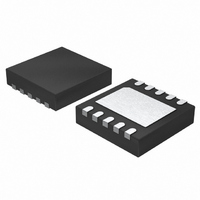
IC 8051 MCU 8K FLASH 10DFN
Manufacturer
Silicon Laboratories Inc
Series
C8051F52xr
Specifications of C8051F521A-IM
Program Memory Type
FLASH
Program Memory Size
8KB (8K x 8)
Package / Case
10-DFN
Core Processor
8051
Core Size
8-Bit
Speed
25MHz
Connectivity
SPI, UART/USART
Peripherals
Brown-out Detect/Reset, POR, PWM, Temp Sensor, WDT
Number Of I /o
6
Ram Size
256 x 8
Voltage - Supply (vcc/vdd)
1.8 V ~ 5.25 V
Data Converters
A/D 6x12b
Oscillator Type
Internal
Operating Temperature
-40°C ~ 125°C
Processor Series
C8051F5x
Core
8051
Data Bus Width
8 bit
Data Ram Size
256 B
Interface Type
SPI/UART
Maximum Clock Frequency
25 MHz
Number Of Programmable I/os
6
Number Of Timers
3
Maximum Operating Temperature
+ 125 C
Mounting Style
SMD/SMT
3rd Party Development Tools
PK51, CA51, A51, ULINK2
Development Tools By Supplier
C8051F500DK
Minimum Operating Temperature
- 40 C
On-chip Adc
6-ch x 12-bit
Lead Free Status / RoHS Status
Lead free / RoHS Compliant
For Use With
336-1488 - KIT DEV C8051F53XA, C8051F52XA770-1006 - ISP 4PORT FOR SILABS C8051F MCU336-1455 - ADAPTER PROGRAM TOOLSTICK F520
Eeprom Size
-
Lead Free Status / Rohs Status
Lead free / RoHS Compliant
Other names
336-1490-5


C8051F52x/F52xA/F53x/F53xA
17.3. LIN Master Mode Operation
The master node is responsible for the scheduling of messages and sends the header of each frame, con-
taining the SYNCH BREAK FIELD, SYNCH FIELD and IDENTIFIER FIELD. The steps to schedule a mes-
sage transmission or reception are listed below.
1. Load the 6-bit Identifier into the LIN0ID register.
2. Load the data length into the LIN0SIZE register. Set the value to the number of data bytes or "1111b" if
3. Set the data direction by setting the TXRX bit (LIN0CTRL.5). Set the bit to 1 to perform a master
4. If performing a master transmit operation, load the data bytes to transmit into the data buffer (LIN0DT1
5. Set the STREQ bit (LIN0CTRL.0) to start the message transfer. The LIN peripheral will schedule the
This code segment shows the procedure to schedule a message in a transmission operation:
The application should perform the following steps when an interrupt is requested.
1. Check the DONE bit (LIN0ST.0) and the ERROR bit (LIN0ST.2).
2. If performing a master receive operation and the transfer was successful, read the received data from
3. If the transfer was not successful, check the error register to determine the kind of error. Further error
4. Set the RSTINT (LIN0CTRL.3) and RSTERR bits (LIN0CTRL.2) to reset the interrupt request and the
168
the data length should be decoded from the identifier. Also, set the checksum type, classic or
enhanced, in the same LIN0SIZE register.
transmit operation, or set the bit to 0 to perform a master receive operation.
to LIN0DT8).
message frame and request an interrupt if the message transfer is successfully completed or if an error
has occurred.
the data buffer.
handling has to be done by the application.
error flags.
LINADDR
LINDATA
LINADDR
LINDATA
LINADDR
LINDATA
LINADDR = 0x00;// Point to Data buffer first byte
for (i=0; i<8; i++)
{
}
LINADDR
LINDATA
LINDATA = i + 0x41;// Load the buffer with ‘A’, ‘B’, ...
LINADDR++;// Increment the address to the next buffer
|=
= 0x08;// Point to LIN0CTRL
= 0x0E;// Point to LIN0ID
= 0x11;// Load the ID, in this example 0x11
= 0x0B;// Point to LIN0SIZE
= ( LINDATA & 0xF0 ) | 0x08; // Load the size with 8
= 0x08;// Point to LIN0CTRL
= 0x01;// Start Request
0x20;// Select to transmit data
Rev. 1.3
Related parts for C8051F521A-IM
Image
Part Number
Description
Manufacturer
Datasheet
Request
R

Part Number:
Description:
SMD/C°/SINGLE-ENDED OUTPUT SILICON OSCILLATOR
Manufacturer:
Silicon Laboratories Inc
Part Number:
Description:
Manufacturer:
Silicon Laboratories Inc
Datasheet:
Part Number:
Description:
N/A N/A/SI4010 AES KEYFOB DEMO WITH LCD RX
Manufacturer:
Silicon Laboratories Inc
Datasheet:
Part Number:
Description:
N/A N/A/SI4010 SIMPLIFIED KEY FOB DEMO WITH LED RX
Manufacturer:
Silicon Laboratories Inc
Datasheet:
Part Number:
Description:
N/A/-40 TO 85 OC/EZLINK MODULE; F930/4432 HIGH BAND (REV E/B1)
Manufacturer:
Silicon Laboratories Inc
Part Number:
Description:
EZLink Module; F930/4432 Low Band (rev e/B1)
Manufacturer:
Silicon Laboratories Inc
Part Number:
Description:
I°/4460 10 DBM RADIO TEST CARD 434 MHZ
Manufacturer:
Silicon Laboratories Inc
Part Number:
Description:
I°/4461 14 DBM RADIO TEST CARD 868 MHZ
Manufacturer:
Silicon Laboratories Inc
Part Number:
Description:
I°/4463 20 DBM RFSWITCH RADIO TEST CARD 460 MHZ
Manufacturer:
Silicon Laboratories Inc
Part Number:
Description:
I°/4463 20 DBM RADIO TEST CARD 868 MHZ
Manufacturer:
Silicon Laboratories Inc
Part Number:
Description:
I°/4463 27 DBM RADIO TEST CARD 868 MHZ
Manufacturer:
Silicon Laboratories Inc
Part Number:
Description:
I°/4463 SKYWORKS 30 DBM RADIO TEST CARD 915 MHZ
Manufacturer:
Silicon Laboratories Inc
Part Number:
Description:
N/A N/A/-40 TO 85 OC/4463 RFMD 30 DBM RADIO TEST CARD 915 MHZ
Manufacturer:
Silicon Laboratories Inc
Part Number:
Description:
I°/4463 20 DBM RADIO TEST CARD 169 MHZ
Manufacturer:
Silicon Laboratories Inc