C8051F521A-IM Silicon Laboratories Inc, C8051F521A-IM Datasheet - Page 210
C8051F521A-IM
Manufacturer Part Number
C8051F521A-IM
Description
IC 8051 MCU 8K FLASH 10DFN
Manufacturer
Silicon Laboratories Inc
Series
C8051F52xr
Specifications of C8051F521A-IM
Program Memory Type
FLASH
Program Memory Size
8KB (8K x 8)
Package / Case
10-DFN
Core Processor
8051
Core Size
8-Bit
Speed
25MHz
Connectivity
SPI, UART/USART
Peripherals
Brown-out Detect/Reset, POR, PWM, Temp Sensor, WDT
Number Of I /o
6
Ram Size
256 x 8
Voltage - Supply (vcc/vdd)
1.8 V ~ 5.25 V
Data Converters
A/D 6x12b
Oscillator Type
Internal
Operating Temperature
-40°C ~ 125°C
Processor Series
C8051F5x
Core
8051
Data Bus Width
8 bit
Data Ram Size
256 B
Interface Type
SPI/UART
Maximum Clock Frequency
25 MHz
Number Of Programmable I/os
6
Number Of Timers
3
Maximum Operating Temperature
+ 125 C
Mounting Style
SMD/SMT
3rd Party Development Tools
PK51, CA51, A51, ULINK2
Development Tools By Supplier
C8051F500DK
Minimum Operating Temperature
- 40 C
On-chip Adc
6-ch x 12-bit
Lead Free Status / RoHS Status
Lead free / RoHS Compliant
For Use With
336-1488 - KIT DEV C8051F53XA, C8051F52XA770-1006 - ISP 4PORT FOR SILABS C8051F MCU336-1455 - ADAPTER PROGRAM TOOLSTICK F520
Eeprom Size
-
Lead Free Status / Rohs Status
Lead free / RoHS Compliant
Other names
336-1490-5


C8051F52x/F52xA/F53x/F53xA
20.2. Reset Pin Behavior
The reset behavior of C8051F52x/F53x differs from C8051F52xA/F53xA devices. The differences affect
the state of the RST pin during a VDD Monitor reset.
On C8051F52x/F53x devices, a V
C8051F52xA/F53xA devices, a V
condition.
20.3. Reset Time Delay
The reset time delay on C8051F52x/F53x devices differs from C8051F52xA/F53xA devices.
On C8051F52x/F53x devices, the reset time delay will be as long as 80 ms following a power-on reset,
meaning it can take up to 80 ms to begin code execution. Subsequent resets will not cause the long delay.
On C8051F52xA/F53xA devices, the startup time is around 350 µs.
20.4. UART Pins
The location of the pins used by the serial UART interface is different between C8051F52x/F53x and
C8051F52xA/F53xA devices.
On C8051F52x/F53x devices, the TX and RX pins used by the UART interface are mapped to the P0.3
(TX) and P0.4 (RX) pins. On C8051F52xA/F53xA, the TX and RX pins used by the UART interface are
mapped to the P0.4 (TX) and P0.5 (RX) pins.
Important Note: On C8051F52xA/53xA devices, the UART pins must be skipped if the UART is enabled
in order for peripherals to appear on port pins beyond the UART on the crossbar. For example, with the
SPI and UART enabled on the crossbar with the SPI on P1.0-P1.3, the UART pins must be skipped using
P0SKIP for the SPI pins to appear correctly.
20.5. LIN
The LIN peripheral behavior in C8051F52x/F53x devices is different than the behavior of
C8051F52xA/F53xA devices. The differences are:
20.5.1. Stop Bit Check
On C8051F52x/F53x devices, the stop bits of the fields in the LIN frame are not checked and no error is
generated if the stop bits could not be sent or received correctly. On C8051F52xA/F53xA devices, the stop
bits are checked, and an error will be generated if the stop bit was not sent or received correctly.
210
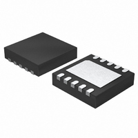
Figure 20.3. Device Package—DFN 10
DD
Monitor reset will pull the RST pin low for the duration of the brownout
DD
520A
BNAB
628+
This character identifies
the device
Monitor reset does not affect the state of the RST pin. On
Rev. 1.3
Related parts for C8051F521A-IM
Image
Part Number
Description
Manufacturer
Datasheet
Request
R

Part Number:
Description:
SMD/C°/SINGLE-ENDED OUTPUT SILICON OSCILLATOR
Manufacturer:
Silicon Laboratories Inc
Part Number:
Description:
Manufacturer:
Silicon Laboratories Inc
Datasheet:
Part Number:
Description:
N/A N/A/SI4010 AES KEYFOB DEMO WITH LCD RX
Manufacturer:
Silicon Laboratories Inc
Datasheet:
Part Number:
Description:
N/A N/A/SI4010 SIMPLIFIED KEY FOB DEMO WITH LED RX
Manufacturer:
Silicon Laboratories Inc
Datasheet:
Part Number:
Description:
N/A/-40 TO 85 OC/EZLINK MODULE; F930/4432 HIGH BAND (REV E/B1)
Manufacturer:
Silicon Laboratories Inc
Part Number:
Description:
EZLink Module; F930/4432 Low Band (rev e/B1)
Manufacturer:
Silicon Laboratories Inc
Part Number:
Description:
I°/4460 10 DBM RADIO TEST CARD 434 MHZ
Manufacturer:
Silicon Laboratories Inc
Part Number:
Description:
I°/4461 14 DBM RADIO TEST CARD 868 MHZ
Manufacturer:
Silicon Laboratories Inc
Part Number:
Description:
I°/4463 20 DBM RFSWITCH RADIO TEST CARD 460 MHZ
Manufacturer:
Silicon Laboratories Inc
Part Number:
Description:
I°/4463 20 DBM RADIO TEST CARD 868 MHZ
Manufacturer:
Silicon Laboratories Inc
Part Number:
Description:
I°/4463 27 DBM RADIO TEST CARD 868 MHZ
Manufacturer:
Silicon Laboratories Inc
Part Number:
Description:
I°/4463 SKYWORKS 30 DBM RADIO TEST CARD 915 MHZ
Manufacturer:
Silicon Laboratories Inc
Part Number:
Description:
N/A N/A/-40 TO 85 OC/4463 RFMD 30 DBM RADIO TEST CARD 915 MHZ
Manufacturer:
Silicon Laboratories Inc
Part Number:
Description:
I°/4463 20 DBM RADIO TEST CARD 169 MHZ
Manufacturer:
Silicon Laboratories Inc