C8051F521A-IM Silicon Laboratories Inc, C8051F521A-IM Datasheet - Page 4
C8051F521A-IM
Manufacturer Part Number
C8051F521A-IM
Description
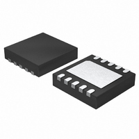
IC 8051 MCU 8K FLASH 10DFN
Manufacturer
Silicon Laboratories Inc
Series
C8051F52xr
Specifications of C8051F521A-IM
Program Memory Type
FLASH
Program Memory Size
8KB (8K x 8)
Package / Case
10-DFN
Core Processor
8051
Core Size
8-Bit
Speed
25MHz
Connectivity
SPI, UART/USART
Peripherals
Brown-out Detect/Reset, POR, PWM, Temp Sensor, WDT
Number Of I /o
6
Ram Size
256 x 8
Voltage - Supply (vcc/vdd)
1.8 V ~ 5.25 V
Data Converters
A/D 6x12b
Oscillator Type
Internal
Operating Temperature
-40°C ~ 125°C
Processor Series
C8051F5x
Core
8051
Data Bus Width
8 bit
Data Ram Size
256 B
Interface Type
SPI/UART
Maximum Clock Frequency
25 MHz
Number Of Programmable I/os
6
Number Of Timers
3
Maximum Operating Temperature
+ 125 C
Mounting Style
SMD/SMT
3rd Party Development Tools
PK51, CA51, A51, ULINK2
Development Tools By Supplier
C8051F500DK
Minimum Operating Temperature
- 40 C
On-chip Adc
6-ch x 12-bit
Lead Free Status / RoHS Status
Lead free / RoHS Compliant
For Use With
336-1488 - KIT DEV C8051F53XA, C8051F52XA770-1006 - ISP 4PORT FOR SILABS C8051F MCU336-1455 - ADAPTER PROGRAM TOOLSTICK F520
Eeprom Size
-
Lead Free Status / Rohs Status
Lead free / RoHS Compliant
Other names
336-1490-5


C8051F52x/F52xA/F53x/F53xA
9. Memory Organization and SFRs............................................................................. 92
10. Interrupt Handler.................................................................................................... 98
11. Reset Sources ...................................................................................................... 106
12. Flash Memory....................................................................................................... 112
13. Port Input/Output ................................................................................................. 119
14. Oscillators ............................................................................................................ 134
4
9.1. Program Memory............................................................................................... 92
9.2. Data Memory ..................................................................................................... 93
9.3. General Purpose Registers ............................................................................... 93
9.4. Bit Addressable Locations ................................................................................. 93
9.5. Stack
9.6. Special Function Registers................................................................................ 93
10.1. MCU Interrupt Sources and Vectors................................................................ 98
10.2. Interrupt Priorities ............................................................................................ 98
10.3. Interrupt Latency.............................................................................................. 98
10.4. Interrupt Register Descriptions ...................................................................... 100
10.5. External Interrupts ......................................................................................... 104
11.1. Power-On Reset ............................................................................................ 107
11.2. Power-Fail Reset / VDD Monitor ................................................................... 107
11.3. External Reset ............................................................................................... 109
11.4. Missing Clock Detector Reset ....................................................................... 109
11.5. Comparator Reset ......................................................................................... 109
11.6. PCA Watchdog Timer Reset ......................................................................... 110
11.7. Flash Error Reset .......................................................................................... 110
11.8. Software Reset .............................................................................................. 110
12.1. Programming The Flash Memory .................................................................. 112
12.2. Flash Write and Erase Guidelines ................................................................. 114
12.3. Non-volatile Data Storage ............................................................................. 116
12.4. Security Options ............................................................................................ 116
13.1. Priority Crossbar Decoder ............................................................................. 121
13.2. Port I/O Initialization ...................................................................................... 125
13.3. General Purpose Port I/O .............................................................................. 127
14.1. Programmable Internal Oscillator .................................................................. 134
14.2. External Oscillator Drive Circuit..................................................................... 138
8.3.2. Stop Mode................................................................................................. 90
8.3.3. Suspend Mode .......................................................................................... 90
12.1.1. Flash Lock and Key Functions .............................................................. 112
12.1.2. Flash Erase Procedure ......................................................................... 113
12.1.3. Flash Write Procedure .......................................................................... 113
12.2.1. V
12.2.2. PSWE Maintenance .............................................................................. 114
12.2.3. System Clock ........................................................................................ 115
14.1.1. Internal Oscillator Suspend Mode ......................................................... 135
14.2.1. Clocking Timers Directly Through the External Oscillator..................... 138
14.2.2. External Crystal Example...................................................................... 138
DD
............................................................................................................ 93
Maintenance and the V
Rev. 1.3
DD
monitor ................................................ 114
Related parts for C8051F521A-IM
Image
Part Number
Description
Manufacturer
Datasheet
Request
R

Part Number:
Description:
SMD/C°/SINGLE-ENDED OUTPUT SILICON OSCILLATOR
Manufacturer:
Silicon Laboratories Inc
Part Number:
Description:
Manufacturer:
Silicon Laboratories Inc
Datasheet:
Part Number:
Description:
N/A N/A/SI4010 AES KEYFOB DEMO WITH LCD RX
Manufacturer:
Silicon Laboratories Inc
Datasheet:
Part Number:
Description:
N/A N/A/SI4010 SIMPLIFIED KEY FOB DEMO WITH LED RX
Manufacturer:
Silicon Laboratories Inc
Datasheet:
Part Number:
Description:
N/A/-40 TO 85 OC/EZLINK MODULE; F930/4432 HIGH BAND (REV E/B1)
Manufacturer:
Silicon Laboratories Inc
Part Number:
Description:
EZLink Module; F930/4432 Low Band (rev e/B1)
Manufacturer:
Silicon Laboratories Inc
Part Number:
Description:
I°/4460 10 DBM RADIO TEST CARD 434 MHZ
Manufacturer:
Silicon Laboratories Inc
Part Number:
Description:
I°/4461 14 DBM RADIO TEST CARD 868 MHZ
Manufacturer:
Silicon Laboratories Inc
Part Number:
Description:
I°/4463 20 DBM RFSWITCH RADIO TEST CARD 460 MHZ
Manufacturer:
Silicon Laboratories Inc
Part Number:
Description:
I°/4463 20 DBM RADIO TEST CARD 868 MHZ
Manufacturer:
Silicon Laboratories Inc
Part Number:
Description:
I°/4463 27 DBM RADIO TEST CARD 868 MHZ
Manufacturer:
Silicon Laboratories Inc
Part Number:
Description:
I°/4463 SKYWORKS 30 DBM RADIO TEST CARD 915 MHZ
Manufacturer:
Silicon Laboratories Inc
Part Number:
Description:
N/A N/A/-40 TO 85 OC/4463 RFMD 30 DBM RADIO TEST CARD 915 MHZ
Manufacturer:
Silicon Laboratories Inc
Part Number:
Description:
I°/4463 20 DBM RADIO TEST CARD 169 MHZ
Manufacturer:
Silicon Laboratories Inc