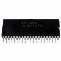
TMP86FH46ANG(Z) Toshiba, TMP86FH46ANG(Z) Datasheet - Page 25

TMP86FH46ANG(Z)
Manufacturer Part Number
TMP86FH46ANG(Z)
Description
IC MCU 8BIT FLASH 16KB 42-SDIP
Manufacturer
Toshiba
Series
TLCS-870/Cr
Datasheet
1.TMP86FH46ANGZ.pdf
(214 pages)
Specifications of TMP86FH46ANG(Z)
Core Processor
870/C
Core Size
8-Bit
Speed
16MHz
Connectivity
SIO, UART/USART
Peripherals
LED, PWM, WDT
Number Of I /o
33
Program Memory Size
16KB (16K x 8)
Program Memory Type
FLASH
Ram Size
512 x 8
Voltage - Supply (vcc/vdd)
2.7 V ~ 5.5 V
Data Converters
A/D 8x10b
Oscillator Type
Internal
Operating Temperature
-40°C ~ 85°C
Package / Case
42-SDIP (0.600", 15.24mm)
Processor Series
TLCS-870
Core
870/C
Data Bus Width
8 bit
Data Ram Size
512 B
Interface Type
SIO, UART
Maximum Clock Frequency
16 MHz
Number Of Programmable I/os
33
Number Of Timers
3
Maximum Operating Temperature
+ 85 C
Mounting Style
Through Hole
Development Tools By Supplier
BMSKTOPAS86FH47(AND), BM1040R0A, BMP86A100010A, BMP86A100010B, BMP86A200010B, BMP86A200020A, BMP86A300010A, BMP86A300020A, BMP86A300030A, SW89CN0-ZCC, SW00MN0-ZCC
Minimum Operating Temperature
- 40 C
On-chip Adc
10 bit, 8 Channel
For Use With
BM1401W0A-G - FLASH WRITER ON-BOARD PROGRAMTMP86C909XB - EMULATION CHIP FOR TMP86F SDIP
Lead Free Status / RoHS Status
Lead free / RoHS Compliant
Eeprom Size
-
Lead Free Status / Rohs Status
Details
Other names
TMP86FH46ANGZ
- Current page: 25 of 214
- Download datasheet (3Mb)
Timing Generator Control Register
Main system clock
2.2.3 Operation Mode Control Circuit
(0036H)
TBTCR
2.2.2.2
2.2.3.1
Note 1: In single clock mode, do not set DV7CK to “1”.
Note 2: Do not set “1” on DV7CK while the low-frequency clock is not operated stably.
Note 3: fc: High-frequency clock [Hz], fs: Low-frequency clock [Hz], *: Don’t care
Note 4: In SLOW1/2 and SLEEP1/2 modes, the DV7CK setting is ineffective, and fs is input to the 7th stage of the divider.
Note 5: When STOP mode is entered from NORMAL1/2 mode, the DV7CK setting is ineffective during the warm-up period after
frequency clocks, and switches the main system clock. There are three operating modes: Single clock mode,
dual clock mode and STOP mode. These modes are controlled by the system control registers (SYSCR1 and
SYSCR2). Figure 2-6 shows the operating mode transition diagram.
State
The operation mode control circuit starts and stops the oscillation circuits for the high-frequency and low-
(DVOEN)
release of STOP mode, and the 6th stage of the divider is input to the 7th stage during this period.
DV7CK
types of instructions for the TLCS-870/C Series: Ranging from 1-cycle instructions which require one
machine cycle for execution to 10-cycle instructions which require 10 machine cycles for execution. A
machine cycle consists of 4 states (S0 to S3), and each state consists of one main system clock.
pins are used as input/output ports. The main-system clock is obtained from the high-frequency clock. In
the single-clock mode, the machine cycle time is 4/fc [s].
7
Machine cycle
Single-clock mode
(1)
Instruction execution and peripheral hardware operation are synchronized with the main system clock.
The minimum instruction execution unit is called an “machine cycle”. There are a total of 10 different
Only the oscillation circuit for the high-frequency clock is used, and P21 (XTIN) and P22 (XTOUT)
The TMP86FH46ANG is placed in this mode after reset.
1/fc or 1/fs [s]
NORMAL1 mode
In this mode, both the CPU core and on-chip peripherals operate using the high-frequency clock.
Selection of input to the 7th stage
of the divider
6
(DVOCK)
S0
5
S1
Machine cycle
DV7CK
Figure 2-5 Machine Cycle
4
(TBTEN)
S2
3
0: fc/2
1: fs
Page 11
8
[Hz]
S3
2
(TBTCK)
1
S0
0
S1
(Initial value: 0000 0000)
S2
TMP86FH46ANG
S3
R/W
Related parts for TMP86FH46ANG(Z)
Image
Part Number
Description
Manufacturer
Datasheet
Request
R
Part Number:
Description:
Toshiba Semiconductor [TOSHIBA IGBT Module Silicon N Channel IGBT]
Manufacturer:
TOSHIBA Semiconductor CORPORATION
Datasheet:
Part Number:
Description:
TOSHIBA GTR MODULE SILICON NPN TRIPLE DIFFUSED TYPE
Manufacturer:
TOSHIBA Semiconductor CORPORATION
Datasheet:
Part Number:
Description:
TOSHIBA GTR Module Silicon N Channel IGBT
Manufacturer:
TOSHIBA Semiconductor CORPORATION
Datasheet:
Part Number:
Description:
TOSHIBA Intelligent Power Module Silicon N Channel IGBT
Manufacturer:
TOSHIBA Semiconductor CORPORATION
Datasheet:
Part Number:
Description:
TOSHIBA INTELLIGENT POWER MODULE SILICON N CHANNEL LGBT
Manufacturer:
TOSHIBA Semiconductor CORPORATION
Datasheet:
Part Number:
Description:
TOSHIBA IGBT Module Silicon N Channel IGBT
Manufacturer:
TOSHIBA Semiconductor CORPORATION
Datasheet:
Part Number:
Description:
TOSHIBA GTR MODULE SILICON N−CHANNEL IGBT
Manufacturer:
TOSHIBA Semiconductor CORPORATION
Datasheet:
Part Number:
Description:
TOSHIBA Intelligent Power Module Silicon N Channel IGBT
Manufacturer:
TOSHIBA Semiconductor CORPORATION
Datasheet:
Part Number:
Description:
TOSHIBA GTR Module Silicon N Channel IGBT
Manufacturer:
TOSHIBA Semiconductor CORPORATION
Datasheet:
Part Number:
Description:
TOSHIBA INTELLIGENT POWER MODULE
Manufacturer:
TOSHIBA Semiconductor CORPORATION
Datasheet:
Part Number:
Description:
TOSHIBA Intelligent Power Module Silicon N Channel IGBT
Manufacturer:
TOSHIBA Semiconductor CORPORATION
Datasheet:
Part Number:
Description:
TOSHIBA Intelligent Power Module Silicon N Channel IGBT
Manufacturer:
TOSHIBA Semiconductor CORPORATION
Datasheet:
Part Number:
Description:
TOSHIBA IGBT Module Silicon N Channel IGBT
Manufacturer:
TOSHIBA Semiconductor CORPORATION
Datasheet:
Part Number:
Description:
TOSHIBA Intelligent Power Module Silicon N Channel IGBT
Manufacturer:
TOSHIBA Semiconductor CORPORATION
Datasheet:
Part Number:
Description:
Toshiba Semiconductor [SILICON N CHANNEL 1GBT]
Manufacturer:
TOSHIBA Semiconductor CORPORATION
Datasheet:


