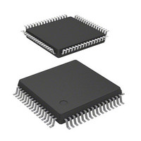
DF71251AD50FPV Renesas Electronics America, DF71251AD50FPV Datasheet - Page 304

DF71251AD50FPV
Manufacturer Part Number
DF71251AD50FPV
Description
MCU RISC FLASH 32K 8K 64LQFP
Manufacturer
Renesas Electronics America
Series
SuperH® SH Tinyr
Datasheet
1.DF71243N50FPV.pdf
(794 pages)
Specifications of DF71251AD50FPV
Core Processor
SH-2
Core Size
32-Bit
Speed
50MHz
Connectivity
SCI
Peripherals
POR, PWM, WDT
Number Of I /o
37
Program Memory Size
32KB (32K x 8)
Program Memory Type
FLASH
Ram Size
8K x 8
Voltage - Supply (vcc/vdd)
4 V ~ 5.5 V
Data Converters
A/D 8x10b
Oscillator Type
External
Operating Temperature
-40°C ~ 85°C
Package / Case
64-LQFP
Lead Free Status / RoHS Status
Lead free / RoHS Compliant
Eeprom Size
-
Available stocks
Company
Part Number
Manufacturer
Quantity
Price
Company:
Part Number:
DF71251AD50FPV
Manufacturer:
Renesas Electronics America
Quantity:
10 000
- Current page: 304 of 794
- Download datasheet (5Mb)
10. Complementary PWM Mode PWM Output Generation Method
Rev. 5.00 Mar. 06, 2009 Page 284 of 770
REJ09B0243-0500
In complementary PWM mode, 3-phase output is performed of PWM waveforms with a non-
overlap time between the positive and negative phases. This non-overlap time is called the
dead time.
A PWM waveform is generated by output of the output level selected in the timer output
control register in the event of a compare-match between a counter and data register. While
TCNTS is counting, data register and temporary register values are simultaneously compared
to create consecutive PWM pulses from 0 to 100%. The relative timing of on and off compare-
match occurrence may vary, but the compare-match that turns off each phase takes precedence
to secure the dead time and ensure that the positive phase and negative phase on times do not
overlap. Figures 9.46 to 9.48 show examples of waveform generation in complementary PWM
mode.
The positive phase/negative phase off timing is generated by a compare-match with the solid-
line counter, and the on timing by a compare-match with the dotted-line counter operating with
a delay of the dead time behind the solid-line counter. In the T1 period, compare-match a that
turns off the negative phase has the highest priority, and compare-matches occurring prior to a
are ignored. In the T2 period, compare-match c that turns off the positive phase has the highest
priority, and compare-matches occurring prior to c are ignored.
In normal cases, compare-matches occur in the order a → b → c → d (or c → d → a' → b'),
as shown in figure 9.46.
If compare-matches deviate from the a → b → c → d order, since the time for which the
negative phase is off is less than twice the dead time, the figure shows the positive phase is not
being turned on. If compare-matches deviate from the c → d → a' → b' order, since the time
for which the positive phase is off is less than twice the dead time, the figure shows the
negative phase is not being turned on.
If compare-match c occurs first following compare-match a, as shown in figure 9.47, compare-
match b is ignored, and the negative phase is turned off by compare-match d. This is because
turning off of the positive phase has priority due to the occurrence of compare-match c
(positive phase off timing) before compare-match b (positive phase on timing) (consequently,
the waveform does not change since the positive phase goes from off to off).
Similarly, in the example in figure 9.48, compare-match a' with the new data in the temporary
register occurs before compare-match c, but other compare-matches occurring up to c, which
turns off the positive phase, are ignored. As a result, the negative phase is not turned on.
Thus, in complementary PWM mode, compare-matches at turn-off timings take precedence,
and turn-on timing compare-matches that occur before a turn-off timing compare-match are
ignored.
Related parts for DF71251AD50FPV
Image
Part Number
Description
Manufacturer
Datasheet
Request
R

Part Number:
Description:
KIT STARTER FOR M16C/29
Manufacturer:
Renesas Electronics America
Datasheet:

Part Number:
Description:
KIT STARTER FOR R8C/2D
Manufacturer:
Renesas Electronics America
Datasheet:

Part Number:
Description:
R0K33062P STARTER KIT
Manufacturer:
Renesas Electronics America
Datasheet:

Part Number:
Description:
KIT STARTER FOR R8C/23 E8A
Manufacturer:
Renesas Electronics America
Datasheet:

Part Number:
Description:
KIT STARTER FOR R8C/25
Manufacturer:
Renesas Electronics America
Datasheet:

Part Number:
Description:
KIT STARTER H8S2456 SHARPE DSPLY
Manufacturer:
Renesas Electronics America
Datasheet:

Part Number:
Description:
KIT STARTER FOR R8C38C
Manufacturer:
Renesas Electronics America
Datasheet:

Part Number:
Description:
KIT STARTER FOR R8C35C
Manufacturer:
Renesas Electronics America
Datasheet:

Part Number:
Description:
KIT STARTER FOR R8CL3AC+LCD APPS
Manufacturer:
Renesas Electronics America
Datasheet:

Part Number:
Description:
KIT STARTER FOR RX610
Manufacturer:
Renesas Electronics America
Datasheet:

Part Number:
Description:
KIT STARTER FOR R32C/118
Manufacturer:
Renesas Electronics America
Datasheet:

Part Number:
Description:
KIT DEV RSK-R8C/26-29
Manufacturer:
Renesas Electronics America
Datasheet:

Part Number:
Description:
KIT STARTER FOR SH7124
Manufacturer:
Renesas Electronics America
Datasheet:

Part Number:
Description:
KIT STARTER FOR H8SX/1622
Manufacturer:
Renesas Electronics America
Datasheet:

Part Number:
Description:
KIT DEV FOR SH7203
Manufacturer:
Renesas Electronics America
Datasheet:


