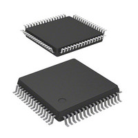
DF71251AD50FPV Renesas Electronics America, DF71251AD50FPV Datasheet - Page 469

DF71251AD50FPV
Manufacturer Part Number
DF71251AD50FPV
Description
MCU RISC FLASH 32K 8K 64LQFP
Manufacturer
Renesas Electronics America
Series
SuperH® SH Tinyr
Datasheet
1.DF71243N50FPV.pdf
(794 pages)
Specifications of DF71251AD50FPV
Core Processor
SH-2
Core Size
32-Bit
Speed
50MHz
Connectivity
SCI
Peripherals
POR, PWM, WDT
Number Of I /o
37
Program Memory Size
32KB (32K x 8)
Program Memory Type
FLASH
Ram Size
8K x 8
Voltage - Supply (vcc/vdd)
4 V ~ 5.5 V
Data Converters
A/D 8x10b
Oscillator Type
External
Operating Temperature
-40°C ~ 85°C
Package / Case
64-LQFP
Lead Free Status / RoHS Status
Lead free / RoHS Compliant
Eeprom Size
-
Available stocks
Company
Part Number
Manufacturer
Quantity
Price
Company:
Part Number:
DF71251AD50FPV
Manufacturer:
Renesas Electronics America
Quantity:
10 000
- Current page: 469 of 794
- Download datasheet (5Mb)
Note : * In simultaneous transmit/receive operation, the TE and RE bits must be cleared to 0 or set to 1
Set the PFC for the external pins to be
Set the RIE, TIE, TEIE, and MPIE bits
Set CKE1 and CKE0 bits in SCSCR
Set TE and RE bits of SCSCR to 1
simultaneously.
TE, and RE bits in SCSCR to 0*
Clear RIE, TIE, TEIE, MPIE,
Set data transfer format in
< Initialization completed>
used (SCK, TXD, RXD)
(TE and RE bits are 0)
1-bit interval elapsed?
Set value in SCBRR
SCSMR, SCSDCR
Figure 12.3 Sample Flowchart for SCI Initialization
Start initialization
in SCSCR
Yes
Wait
No
[1]
[2]
[3]
[4]
[5]
[1] Set the clock selection in SCSCR.
[2] Set the data transfer format in SCSMR
[3] Write a value corresponding to the bit
[4] Set PFC of the external pin used. Set
[5] Set the TE bit or RE bit in SCSCR to 1.*
and SCSDCR.
rate to SCBRR. Not necessary if an
external clock is used.
RXD input during receiving and TXD
output during transmitting. Set SCK
input/output according to contents set by
CKE1 and CKE0. When CKE1 and
CKE0 are 0 in asynchronous mode,
setting the SCK pin is unnecessary.
Outputting clocks from the SCK pin
starts at synchronous clock output
setting.
Also make settings of the RIE, TIE,
TEIE, and MPIE bits. At this time, the
TXD, RXD, and SCK pins are ready to
be used. The TXD pin is in a mark state
during transmitting, and RXD pin is in an
idle state for waiting the start bit during
receiving.
Rev. 5.00 Mar. 06, 2009 Page 449 of 770
REJ09B0243-0500
Related parts for DF71251AD50FPV
Image
Part Number
Description
Manufacturer
Datasheet
Request
R

Part Number:
Description:
KIT STARTER FOR M16C/29
Manufacturer:
Renesas Electronics America
Datasheet:

Part Number:
Description:
KIT STARTER FOR R8C/2D
Manufacturer:
Renesas Electronics America
Datasheet:

Part Number:
Description:
R0K33062P STARTER KIT
Manufacturer:
Renesas Electronics America
Datasheet:

Part Number:
Description:
KIT STARTER FOR R8C/23 E8A
Manufacturer:
Renesas Electronics America
Datasheet:

Part Number:
Description:
KIT STARTER FOR R8C/25
Manufacturer:
Renesas Electronics America
Datasheet:

Part Number:
Description:
KIT STARTER H8S2456 SHARPE DSPLY
Manufacturer:
Renesas Electronics America
Datasheet:

Part Number:
Description:
KIT STARTER FOR R8C38C
Manufacturer:
Renesas Electronics America
Datasheet:

Part Number:
Description:
KIT STARTER FOR R8C35C
Manufacturer:
Renesas Electronics America
Datasheet:

Part Number:
Description:
KIT STARTER FOR R8CL3AC+LCD APPS
Manufacturer:
Renesas Electronics America
Datasheet:

Part Number:
Description:
KIT STARTER FOR RX610
Manufacturer:
Renesas Electronics America
Datasheet:

Part Number:
Description:
KIT STARTER FOR R32C/118
Manufacturer:
Renesas Electronics America
Datasheet:

Part Number:
Description:
KIT DEV RSK-R8C/26-29
Manufacturer:
Renesas Electronics America
Datasheet:

Part Number:
Description:
KIT STARTER FOR SH7124
Manufacturer:
Renesas Electronics America
Datasheet:

Part Number:
Description:
KIT STARTER FOR H8SX/1622
Manufacturer:
Renesas Electronics America
Datasheet:

Part Number:
Description:
KIT DEV FOR SH7203
Manufacturer:
Renesas Electronics America
Datasheet:


