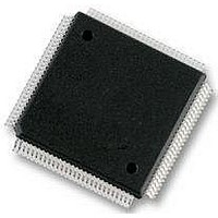
MC912D60CCPVE Freescale Semiconductor, MC912D60CCPVE Datasheet - Page 50

MC912D60CCPVE
Manufacturer Part Number
MC912D60CCPVE
Description
IC MCU 16BIT 112-LQFP
Manufacturer
Freescale Semiconductor
Series
HC12r
Datasheet
1.MC912D60ACFUE8.pdf
(460 pages)
Specifications of MC912D60CCPVE
Core Processor
CPU12
Core Size
16-Bit
Speed
8MHz
Connectivity
CAN, MI Bus, SCI, SPI
Peripherals
POR, PWM, WDT
Number Of I /o
68
Program Memory Size
60KB (60K x 8)
Program Memory Type
FLASH
Eeprom Size
1K x 8
Ram Size
2K x 8
Voltage - Supply (vcc/vdd)
4.5 V ~ 5.5 V
Data Converters
A/D 16x8/10b
Oscillator Type
Internal
Operating Temperature
-40°C ~ 85°C
Package / Case
112-LQFP
Processor Series
HC912D
Core
HC12
Data Bus Width
16 bit
Data Ram Size
2 KB
Interface Type
CAN, SCI, SPI
Maximum Clock Frequency
8 MHz
Number Of Programmable I/os
86
Maximum Operating Temperature
+ 85 C
Mounting Style
SMD/SMT
3rd Party Development Tools
EWHCS12
Minimum Operating Temperature
- 40 C
On-chip Adc
10 bit, 8 Channel
Lead Free Status / RoHS Status
Lead free / RoHS Compliant
Available stocks
Company
Part Number
Manufacturer
Quantity
Price
Company:
Part Number:
MC912D60CCPVE
Manufacturer:
FREESCAL
Quantity:
203
Company:
Part Number:
MC912D60CCPVE
Manufacturer:
Freescale Semiconductor
Quantity:
10 000
- Current page: 50 of 460
- Download datasheet (5Mb)
Pinout and Signal Descriptions
3.5.13 Inverted ECLK (ECLK)
3.5.14 Calibration reference (CAL)
3.5.15 Clock generation module test (CGMTST)
3.5.16 TEST
Technical Data
50
Pin Name
RESET
EXTAL
XTAL
80-pin
35
36
34
Pin Number
Table 3-2. MC68HC912D60A Signal Description Summary
112-pin
The ECLK pin (PE7) can be used to latch the address for de-
multiplexing. It has the same behavior as the ECLK, except is inverted.
In expanded modes this pin is used to enable the drive control of external
buses during external reads. Use of the ECLK is controlled by the NDBE
and DBENE bits in the PEAR register.
The CAL pin (PE7) is the output of the Slow Mode programmable clock
divider, SLWCLK, and is used as a calibration reference. The SLWCLK
frequency is equal to the crystal frequency out of reset and always has
a 50% duty. If the DBE function is enabled it will override the enabled
CAL output. The CAL pin output is disabled by clearing CALE bit in the
PEAR register.
The CGMTST pin (PE6) is the output of the clocks tested when CGMTE
bit is set in PEAR register. The PIPOE bit must be cleared for the clocks
to be tested.
This pin is used for factory test purposes. It is recommended that this
pin is not connected in the application, but it may be bonded to 5.5 V max
without issue. Never apply voltage higher than 5.5 V to this pin.
47
48
46
Crystal driver and external clock input pins.
An active low bidirectional control signal, RESET acts as an input to
initialize the MCU to a known start-up state, and an output when COP or
clock monitor causes a reset.
Pinout and Signal Descriptions
Description
MC68HC912D60A — Rev. 3.1
Freescale Semiconductor
Related parts for MC912D60CCPVE
Image
Part Number
Description
Manufacturer
Datasheet
Request
R
Part Number:
Description:
Manufacturer:
Freescale Semiconductor, Inc
Datasheet:
Part Number:
Description:
Manufacturer:
Freescale Semiconductor, Inc
Datasheet:
Part Number:
Description:
Manufacturer:
Freescale Semiconductor, Inc
Datasheet:
Part Number:
Description:
Manufacturer:
Freescale Semiconductor, Inc
Datasheet:
Part Number:
Description:
Manufacturer:
Freescale Semiconductor, Inc
Datasheet:
Part Number:
Description:
Manufacturer:
Freescale Semiconductor, Inc
Datasheet:
Part Number:
Description:
Manufacturer:
Freescale Semiconductor, Inc
Datasheet:
Part Number:
Description:
Manufacturer:
Freescale Semiconductor, Inc
Datasheet:
Part Number:
Description:
Manufacturer:
Freescale Semiconductor, Inc
Datasheet:
Part Number:
Description:
Manufacturer:
Freescale Semiconductor, Inc
Datasheet:
Part Number:
Description:
Manufacturer:
Freescale Semiconductor, Inc
Datasheet:
Part Number:
Description:
Manufacturer:
Freescale Semiconductor, Inc
Datasheet:
Part Number:
Description:
Manufacturer:
Freescale Semiconductor, Inc
Datasheet:
Part Number:
Description:
Manufacturer:
Freescale Semiconductor, Inc
Datasheet:
Part Number:
Description:
Manufacturer:
Freescale Semiconductor, Inc
Datasheet:


