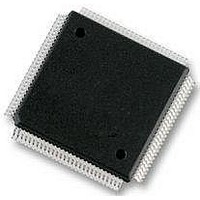
MC912D60CCPVE Freescale Semiconductor, MC912D60CCPVE Datasheet - Page 93

MC912D60CCPVE
Manufacturer Part Number
MC912D60CCPVE
Description
IC MCU 16BIT 112-LQFP
Manufacturer
Freescale Semiconductor
Series
HC12r
Datasheet
1.MC912D60ACFUE8.pdf
(460 pages)
Specifications of MC912D60CCPVE
Core Processor
CPU12
Core Size
16-Bit
Speed
8MHz
Connectivity
CAN, MI Bus, SCI, SPI
Peripherals
POR, PWM, WDT
Number Of I /o
68
Program Memory Size
60KB (60K x 8)
Program Memory Type
FLASH
Eeprom Size
1K x 8
Ram Size
2K x 8
Voltage - Supply (vcc/vdd)
4.5 V ~ 5.5 V
Data Converters
A/D 16x8/10b
Oscillator Type
Internal
Operating Temperature
-40°C ~ 85°C
Package / Case
112-LQFP
Processor Series
HC912D
Core
HC12
Data Bus Width
16 bit
Data Ram Size
2 KB
Interface Type
CAN, SCI, SPI
Maximum Clock Frequency
8 MHz
Number Of Programmable I/os
86
Maximum Operating Temperature
+ 85 C
Mounting Style
SMD/SMT
3rd Party Development Tools
EWHCS12
Minimum Operating Temperature
- 40 C
On-chip Adc
10 bit, 8 Channel
Lead Free Status / RoHS Status
Lead free / RoHS Compliant
Available stocks
Company
Part Number
Manufacturer
Quantity
Price
Company:
Part Number:
MC912D60CCPVE
Manufacturer:
FREESCAL
Quantity:
203
Company:
Part Number:
MC912D60CCPVE
Manufacturer:
Freescale Semiconductor
Quantity:
10 000
- Current page: 93 of 460
- Download datasheet (5Mb)
MC68HC912D60A — Rev. 3.1
Freescale Semiconductor
RDWE — Read/Write Enable
CALE — Calibration Reference Enable
DBENE — DBE or Inverted E Clock on Port E[7]
Normal: write once; Special: write anytime EXCEPT the first time.
Read anytime. This bit has no effect in single-chip modes.
R/W is used for external writes. After reset in normal expanded mode,
it is disabled. If needed it should be enabled before any external
writes.
Read and write anytime.
Normal modes: write once. Special modes: write anytime EXCEPT
the first; read anytime.
DBENE controls which signal is output on PE7 when NDBE control bit
is cleared. The inverted ECLK output can be used to latch the address
for demultiplexing. It has the same behaviour as the ECLK, except it
is inverted. Please note that in the case of idle expansion bus, the ‘not
ECLK’ signal could stay high for many cycles.
The DBNE bit has no effect in single chip or peripheral modes and
PE7 is defaulted to the CAL function if the CALE bit is set in the PEAR
register or to an I/O otherwise.
0 = PE2 is a general-purpose I/O pin.
1 = PE2 is configured as the R/W pin. In single chip modes, RDWE
0 = Calibration reference is disabled and PE7 is general-purpose
1 = Calibration reference is enabled on PE7 in single chip and
0 = PE7 pin used for DBE external control of data enable on
1 = PE7 pin used for inverted ECLK output in expanded modes
has no effect and PE2 is a general-purpose I/O pin.
I/O in single chip or peripheral modes or if the NDBE bit is set.
peripheral modes or if the NDBE bit is set.
memories in expanded modes when NDBE = 0
when NDBE = 0
Bus Control and Input/Output
Bus Control and Input/Output
Technical Data
Registers
93
Related parts for MC912D60CCPVE
Image
Part Number
Description
Manufacturer
Datasheet
Request
R
Part Number:
Description:
Manufacturer:
Freescale Semiconductor, Inc
Datasheet:
Part Number:
Description:
Manufacturer:
Freescale Semiconductor, Inc
Datasheet:
Part Number:
Description:
Manufacturer:
Freescale Semiconductor, Inc
Datasheet:
Part Number:
Description:
Manufacturer:
Freescale Semiconductor, Inc
Datasheet:
Part Number:
Description:
Manufacturer:
Freescale Semiconductor, Inc
Datasheet:
Part Number:
Description:
Manufacturer:
Freescale Semiconductor, Inc
Datasheet:
Part Number:
Description:
Manufacturer:
Freescale Semiconductor, Inc
Datasheet:
Part Number:
Description:
Manufacturer:
Freescale Semiconductor, Inc
Datasheet:
Part Number:
Description:
Manufacturer:
Freescale Semiconductor, Inc
Datasheet:
Part Number:
Description:
Manufacturer:
Freescale Semiconductor, Inc
Datasheet:
Part Number:
Description:
Manufacturer:
Freescale Semiconductor, Inc
Datasheet:
Part Number:
Description:
Manufacturer:
Freescale Semiconductor, Inc
Datasheet:
Part Number:
Description:
Manufacturer:
Freescale Semiconductor, Inc
Datasheet:
Part Number:
Description:
Manufacturer:
Freescale Semiconductor, Inc
Datasheet:
Part Number:
Description:
Manufacturer:
Freescale Semiconductor, Inc
Datasheet:


