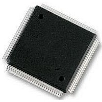
MC912D60CCPVE Freescale Semiconductor, MC912D60CCPVE Datasheet - Page 55

MC912D60CCPVE
Manufacturer Part Number
MC912D60CCPVE
Description
IC MCU 16BIT 112-LQFP
Manufacturer
Freescale Semiconductor
Series
HC12r
Datasheet
1.MC912D60ACFUE8.pdf
(460 pages)
Specifications of MC912D60CCPVE
Core Processor
CPU12
Core Size
16-Bit
Speed
8MHz
Connectivity
CAN, MI Bus, SCI, SPI
Peripherals
POR, PWM, WDT
Number Of I /o
68
Program Memory Size
60KB (60K x 8)
Program Memory Type
FLASH
Eeprom Size
1K x 8
Ram Size
2K x 8
Voltage - Supply (vcc/vdd)
4.5 V ~ 5.5 V
Data Converters
A/D 16x8/10b
Oscillator Type
Internal
Operating Temperature
-40°C ~ 85°C
Package / Case
112-LQFP
Processor Series
HC912D
Core
HC12
Data Bus Width
16 bit
Data Ram Size
2 KB
Interface Type
CAN, SCI, SPI
Maximum Clock Frequency
8 MHz
Number Of Programmable I/os
86
Maximum Operating Temperature
+ 85 C
Mounting Style
SMD/SMT
3rd Party Development Tools
EWHCS12
Minimum Operating Temperature
- 40 C
On-chip Adc
10 bit, 8 Channel
Lead Free Status / RoHS Status
Lead free / RoHS Compliant
Available stocks
Company
Part Number
Manufacturer
Quantity
Price
Company:
Part Number:
MC912D60CCPVE
Manufacturer:
FREESCAL
Quantity:
203
Company:
Part Number:
MC912D60CCPVE
Manufacturer:
Freescale Semiconductor
Quantity:
10 000
- Current page: 55 of 460
- Download datasheet (5Mb)
3.6.4 Port G
3.6.5 Port H
MC68HC912D60A — Rev. 3.1
Freescale Semiconductor
Port G pins are used for key wake-ups that can be used with the pins
configured as inputs or outputs. The key wake-ups are triggered with a
falling edge signal (KWPG). An interrupt is generated if the
corresponding bit is enabled (KWIEG). If any of the interrupts is not
enabled, the corresponding pin can be used as a general purpose I/O
pin. Refer to
Register DDRG determines pin direction of port G when used for
general-purpose I/O. When DDRG bits are set, the corresponding pin is
configured for output. On reset the DDRG bits are cleared and the
corresponding pin is configured for input.
Port PGUPD determines what type of resistive load is used for port G
input pins when PUPG bit is set in the PUCR register. When PGUPD pin
is low, it loads a pull-down in all port G input pins. When PGUPD pin is
high, it loads a pull-up in all port G input pins.
In 80-pin version, the PGUPD is connected internally to VDD. The PG4
will have a pull-up. All port G pins should either be defined as outputs or
have their pull-ups enabled.
Setting the RDPG bit in register RDRIV causes all port G outputs to have
reduced drive level. RDRIV can be written once after reset. RDRIV is not
in the address map in peripheral mode. Refer to
Input/Output.
Port H pins are used for key wake-ups that can be used with the pins
configured as inputs or outputs. The key wake-ups are triggered with a
falling edge signal (KWPH). An interrupt is generated if the
corresponding bit is enabled (KWIEH). If any of the interrupts is not
enabled, the corresponding pin can be used as a general purpose I/O
pin. Refer to
Register DDRH determines pin direction of Port H when used for
general-purpose I/O. When DDRH bits are set, the corresponding pin is
Pinout and Signal Descriptions
I/O Ports with Key
I/O Ports with Key
Wake-up.
Wake-up.
Pinout and Signal Descriptions
Bus Control and
Technical Data
Port Signals
55
Related parts for MC912D60CCPVE
Image
Part Number
Description
Manufacturer
Datasheet
Request
R
Part Number:
Description:
Manufacturer:
Freescale Semiconductor, Inc
Datasheet:
Part Number:
Description:
Manufacturer:
Freescale Semiconductor, Inc
Datasheet:
Part Number:
Description:
Manufacturer:
Freescale Semiconductor, Inc
Datasheet:
Part Number:
Description:
Manufacturer:
Freescale Semiconductor, Inc
Datasheet:
Part Number:
Description:
Manufacturer:
Freescale Semiconductor, Inc
Datasheet:
Part Number:
Description:
Manufacturer:
Freescale Semiconductor, Inc
Datasheet:
Part Number:
Description:
Manufacturer:
Freescale Semiconductor, Inc
Datasheet:
Part Number:
Description:
Manufacturer:
Freescale Semiconductor, Inc
Datasheet:
Part Number:
Description:
Manufacturer:
Freescale Semiconductor, Inc
Datasheet:
Part Number:
Description:
Manufacturer:
Freescale Semiconductor, Inc
Datasheet:
Part Number:
Description:
Manufacturer:
Freescale Semiconductor, Inc
Datasheet:
Part Number:
Description:
Manufacturer:
Freescale Semiconductor, Inc
Datasheet:
Part Number:
Description:
Manufacturer:
Freescale Semiconductor, Inc
Datasheet:
Part Number:
Description:
Manufacturer:
Freescale Semiconductor, Inc
Datasheet:
Part Number:
Description:
Manufacturer:
Freescale Semiconductor, Inc
Datasheet:


