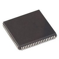
HD64F3337YCP16V Renesas Electronics America, HD64F3337YCP16V Datasheet - Page 181

HD64F3337YCP16V
Manufacturer Part Number
HD64F3337YCP16V
Description
MCU 3/5V 60K PB-FREE 84-PLCC
Manufacturer
Renesas Electronics America
Series
H8® H8/300r
Specifications of HD64F3337YCP16V
Core Size
8-Bit
Program Memory Size
60KB (60K x 8)
Oscillator Type
Internal
Core Processor
H8/300
Speed
16MHz
Connectivity
Host Interface, I²C, SCI
Peripherals
POR, PWM, WDT
Number Of I /o
74
Program Memory Type
FLASH
Ram Size
2K x 8
Voltage - Supply (vcc/vdd)
4.5 V ~ 5.5 V
Data Converters
A/D 8x10b; D/A 2x8b
Operating Temperature
-20°C ~ 75°C
Package / Case
84-PLCC
No. Of I/o's
74
Ram Memory Size
1KB
Cpu Speed
16MHz
No. Of Timers
6
No. Of Pwm Channels
2
Digital Ic Case Style
PLCC
Controller Family/series
H8/300
Rohs Compliant
Yes
Lead Free Status / RoHS Status
Lead free / RoHS Compliant
Eeprom Size
-
Lead Free Status / RoHS Status
Lead free / RoHS Compliant, Lead free / RoHS Compliant
Available stocks
Company
Part Number
Manufacturer
Quantity
Price
Company:
Part Number:
HD64F3337YCP16V
Manufacturer:
COILMASTER
Quantity:
30 000
Company:
Part Number:
HD64F3337YCP16V
Manufacturer:
Renesas Electronics America
Quantity:
10 000
- Current page: 181 of 747
- Download datasheet (4Mb)
7.10
7.10.1
Port 9 is an 8-bit input/output port that is multiplexed with interrupt input pins
input/output pins for bus control signals (RD, WR, AS, WAIT), an input pin (ADTRG) for the
A/D converter, an output pin (ø) for the system clock, host interface (HIF) input pins (ECS
EIOW), and the I
9. The functions of pins P9
P9
Pins in port 9 can drive one TTL load and a 90-pF capacitive load. They can also drive a
darlington pair.
Pin 9
Note: *1 The SDA pin functions applies to the H8/3337 Series only. The H8/3397 Series does
2
Port 9
are unaffected by bit STAC.
7
can drive a bus buffer. For details, see section 13, I
Port 9
Overview
not support a I
2
C data input/output pin (SDA). Figure 7.17 shows the pin configuration of port
Port 9 pins
P9
P9
P9
P9
P9
P9
7
6
5
4
3
2
2
/WAIT/SDA
/ø
/AS
/WR
/RD
/IRQ
C bus interface, and therefore has no SDA pin functions.
1
and P9
Figure 7.17 Port 9 Pin Configuration
0
0
are configured according to bit STAC in STCR. Pins P9
*1
Pin configuration in mode 3 (single-chip mode)
P9
P9
P9
P9
P9
P9
7
6
5
4
3
2
(input/output)/SDA
(input)/ø (output)
(input/output)
(input/output)
(input/output)
(input/output)/IRQ
Pin configuration in mode 1 (expanded mode
with on-chip ROM disabled) and mode 2
(expanded mode with on-chip ROM enabled)
P9
ø (output)
AS (output)
WR (output)
RD (output)
P9
7
2
(input/output)/IRQ
(input/output)/WAIT (input)/SDA (input/output)
2
C Bus Interface.
0
*1
(input)
(input/output)
0
(input)
(
IRQ
0
to IRQ
2
,
2
7
),
to
151
Related parts for HD64F3337YCP16V
Image
Part Number
Description
Manufacturer
Datasheet
Request
R

Part Number:
Description:
KIT STARTER FOR M16C/29
Manufacturer:
Renesas Electronics America
Datasheet:

Part Number:
Description:
KIT STARTER FOR R8C/2D
Manufacturer:
Renesas Electronics America
Datasheet:

Part Number:
Description:
R0K33062P STARTER KIT
Manufacturer:
Renesas Electronics America
Datasheet:

Part Number:
Description:
KIT STARTER FOR R8C/23 E8A
Manufacturer:
Renesas Electronics America
Datasheet:

Part Number:
Description:
KIT STARTER FOR R8C/25
Manufacturer:
Renesas Electronics America
Datasheet:

Part Number:
Description:
KIT STARTER H8S2456 SHARPE DSPLY
Manufacturer:
Renesas Electronics America
Datasheet:

Part Number:
Description:
KIT STARTER FOR R8C38C
Manufacturer:
Renesas Electronics America
Datasheet:

Part Number:
Description:
KIT STARTER FOR R8C35C
Manufacturer:
Renesas Electronics America
Datasheet:

Part Number:
Description:
KIT STARTER FOR R8CL3AC+LCD APPS
Manufacturer:
Renesas Electronics America
Datasheet:

Part Number:
Description:
KIT STARTER FOR RX610
Manufacturer:
Renesas Electronics America
Datasheet:

Part Number:
Description:
KIT STARTER FOR R32C/118
Manufacturer:
Renesas Electronics America
Datasheet:

Part Number:
Description:
KIT DEV RSK-R8C/26-29
Manufacturer:
Renesas Electronics America
Datasheet:

Part Number:
Description:
KIT STARTER FOR SH7124
Manufacturer:
Renesas Electronics America
Datasheet:

Part Number:
Description:
KIT STARTER FOR H8SX/1622
Manufacturer:
Renesas Electronics America
Datasheet:

Part Number:
Description:
KIT DEV FOR SH7203
Manufacturer:
Renesas Electronics America
Datasheet:


