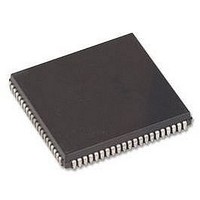
HD64F3337YCP16V Renesas Electronics America, HD64F3337YCP16V Datasheet - Page 292

HD64F3337YCP16V
Manufacturer Part Number
HD64F3337YCP16V
Description
MCU 3/5V 60K PB-FREE 84-PLCC
Manufacturer
Renesas Electronics America
Series
H8® H8/300r
Specifications of HD64F3337YCP16V
Core Size
8-Bit
Program Memory Size
60KB (60K x 8)
Oscillator Type
Internal
Core Processor
H8/300
Speed
16MHz
Connectivity
Host Interface, I²C, SCI
Peripherals
POR, PWM, WDT
Number Of I /o
74
Program Memory Type
FLASH
Ram Size
2K x 8
Voltage - Supply (vcc/vdd)
4.5 V ~ 5.5 V
Data Converters
A/D 8x10b; D/A 2x8b
Operating Temperature
-20°C ~ 75°C
Package / Case
84-PLCC
No. Of I/o's
74
Ram Memory Size
1KB
Cpu Speed
16MHz
No. Of Timers
6
No. Of Pwm Channels
2
Digital Ic Case Style
PLCC
Controller Family/series
H8/300
Rohs Compliant
Yes
Lead Free Status / RoHS Status
Lead free / RoHS Compliant
Eeprom Size
-
Lead Free Status / RoHS Status
Lead free / RoHS Compliant, Lead free / RoHS Compliant
Available stocks
Company
Part Number
Manufacturer
Quantity
Price
Company:
Part Number:
HD64F3337YCP16V
Manufacturer:
COILMASTER
Quantity:
30 000
Company:
Part Number:
HD64F3337YCP16V
Manufacturer:
Renesas Electronics America
Quantity:
10 000
- Current page: 292 of 747
- Download datasheet (4Mb)
262
1
2
3
4
Start transmitting or receiving
Set CKE1 and CKE0 bits in
and set RIE, TIE, TEIE, and
Set TE or RE to 1 in SCR,
SCR (leaving TE and RE
Clear TE and RE bits to
Select communication
MPIE as necessary
Set value in BRR
format in SMR
cleared to 0)
1 bit interval
Initialization
0 in SCR
elapsed?
Figure 12.4 Sample Flowchart for SCI Initialization
Yes
No
1.
2.
3.
4.
Select interrupts and the clock source in the
serial control register (SCR). Leave TE and RE
cleared to 0. If clock output is selected, in
asynchronous mode, clock output starts
immediately after the setting is made in SCR.
Select the communication format in the serial
mode register (SMR).
Write the value corresponding to the bit rate in
the bit rate register (BRR). This step is not
necessary when an external clock is used.
Wait for at least the interval required to transmit
or receive one bit, then set TE or RE in the serial
control register (SCR). Setting TE or RE enables
the SCI to use the TxD or RxD pin.
Also set the RIE, TIE, TEIE, and MPIE bits as
necessary to enable interrupts. The initial states
are the mark transmit state, and the idle receive
state (waiting for a start bit).
Related parts for HD64F3337YCP16V
Image
Part Number
Description
Manufacturer
Datasheet
Request
R

Part Number:
Description:
KIT STARTER FOR M16C/29
Manufacturer:
Renesas Electronics America
Datasheet:

Part Number:
Description:
KIT STARTER FOR R8C/2D
Manufacturer:
Renesas Electronics America
Datasheet:

Part Number:
Description:
R0K33062P STARTER KIT
Manufacturer:
Renesas Electronics America
Datasheet:

Part Number:
Description:
KIT STARTER FOR R8C/23 E8A
Manufacturer:
Renesas Electronics America
Datasheet:

Part Number:
Description:
KIT STARTER FOR R8C/25
Manufacturer:
Renesas Electronics America
Datasheet:

Part Number:
Description:
KIT STARTER H8S2456 SHARPE DSPLY
Manufacturer:
Renesas Electronics America
Datasheet:

Part Number:
Description:
KIT STARTER FOR R8C38C
Manufacturer:
Renesas Electronics America
Datasheet:

Part Number:
Description:
KIT STARTER FOR R8C35C
Manufacturer:
Renesas Electronics America
Datasheet:

Part Number:
Description:
KIT STARTER FOR R8CL3AC+LCD APPS
Manufacturer:
Renesas Electronics America
Datasheet:

Part Number:
Description:
KIT STARTER FOR RX610
Manufacturer:
Renesas Electronics America
Datasheet:

Part Number:
Description:
KIT STARTER FOR R32C/118
Manufacturer:
Renesas Electronics America
Datasheet:

Part Number:
Description:
KIT DEV RSK-R8C/26-29
Manufacturer:
Renesas Electronics America
Datasheet:

Part Number:
Description:
KIT STARTER FOR SH7124
Manufacturer:
Renesas Electronics America
Datasheet:

Part Number:
Description:
KIT STARTER FOR H8SX/1622
Manufacturer:
Renesas Electronics America
Datasheet:

Part Number:
Description:
KIT DEV FOR SH7203
Manufacturer:
Renesas Electronics America
Datasheet:


