M30835FJGP#U5 Renesas Electronics America, M30835FJGP#U5 Datasheet - Page 270
M30835FJGP#U5
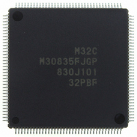
Manufacturer Part Number
M30835FJGP#U5
Description
IC M32C/83 MCU FLASH 144LQFP
Manufacturer
Renesas Electronics America
Series
M16C™ M32C/80r
Datasheets
1.M3087BFLGPU3.pdf
(364 pages)
2.M30833FJGPU3.pdf
(96 pages)
3.M30833FJGPU3.pdf
(529 pages)
Specifications of M30835FJGP#U5
Core Processor
M32C/80
Core Size
16/32-Bit
Speed
32MHz
Connectivity
CAN, I²C, IEBus, SIO, UART/USART
Peripherals
DMA, WDT
Number Of I /o
121
Program Memory Size
512KB (512K x 8)
Program Memory Type
FLASH
Ram Size
31K x 8
Voltage - Supply (vcc/vdd)
3 V ~ 5.5 V
Data Converters
A/D 34x10b, D/A 2x8b
Oscillator Type
Internal
Operating Temperature
-20°C ~ 85°C
Package / Case
144-LQFP
For Use With
R0K330879S001BE - KIT DEV RSK M32C/87R0K330879S000BE - KIT DEV RSK M32C/87
Lead Free Status / RoHS Status
Lead free / RoHS Compliant
Eeprom Size
-
Available stocks
Company
Part Number
Manufacturer
Quantity
Price

Part Number:
M30835FJGP#U5M30835FJGP#U3
Manufacturer:
Renesas Electronics America
Quantity:
10 000


R
R
M
e
E
20. X/Y Conversion
3
. v
J
Figure 20.1 XYC Register
2
0
1
The X/Y conversion rotates a 16 x 16 matrix data by 90 degrees and inverses high-order bits and low-order
bits of a 16-bit data. Figure 20.1 shows the XYC register.
The 16-bit XiR register (i=0 to 15) and 16-bit YjR register (j=0 to 15) are allocated to the same address. The
XiR register is a write-only register, while the YjR register is a read-only register. Access the XiR and YjR
registers from an even address in 16-bit units. Performance cannot be guaranteed if the XiR and YiR
registers are accessed in 8-bit units.
9
C
3 .
B
8 /
0
1
3
0
3
J
G
4
a
0 -
n
o r
X/Y Control Register
3 .
b7
1
u
, 1
3
p
1
b6
2
(
M
0
b5
0
3
6
2
b4
C
Page 245
8 /
b3
, 3
b2
M
3
b1
2
C
f o
b0
8 /
4
3
8
(b7 - b2)
Symbol
) T
8
XYC0
XYC1
Bit
Symbol
XYC
Read-Mode Set Bit
Write-Mode Set Bit
Noting is assigned. When write, set to "0".
When read, its content is indeterminate.
Bit Name
Address
02E0
16
0 : Data conversion
1 : No data conversion
0 : No bit alignment conversion
1 : Bit alignment conversion
After Reset
XXXX XX00
Function
2
20. XY Conversion
RW
RW
RW
Related parts for M30835FJGP#U5
Image
Part Number
Description
Manufacturer
Datasheet
Request
R

Part Number:
Description:
KIT STARTER FOR M16C/29
Manufacturer:
Renesas Electronics America
Datasheet:

Part Number:
Description:
KIT STARTER FOR R8C/2D
Manufacturer:
Renesas Electronics America
Datasheet:

Part Number:
Description:
R0K33062P STARTER KIT
Manufacturer:
Renesas Electronics America
Datasheet:

Part Number:
Description:
KIT STARTER FOR R8C/23 E8A
Manufacturer:
Renesas Electronics America
Datasheet:

Part Number:
Description:
KIT STARTER FOR R8C/25
Manufacturer:
Renesas Electronics America
Datasheet:

Part Number:
Description:
KIT STARTER H8S2456 SHARPE DSPLY
Manufacturer:
Renesas Electronics America
Datasheet:

Part Number:
Description:
KIT STARTER FOR R8C38C
Manufacturer:
Renesas Electronics America
Datasheet:

Part Number:
Description:
KIT STARTER FOR R8C35C
Manufacturer:
Renesas Electronics America
Datasheet:

Part Number:
Description:
KIT STARTER FOR R8CL3AC+LCD APPS
Manufacturer:
Renesas Electronics America
Datasheet:
Part Number:
Description:
KIT STARTER FOR RX610
Manufacturer:
Renesas Electronics America
Datasheet:

Part Number:
Description:
KIT STARTER FOR R32C/118
Manufacturer:
Renesas Electronics America
Datasheet:

Part Number:
Description:
KIT DEV RSK-R8C/26-29
Manufacturer:
Renesas Electronics America
Datasheet:

Part Number:
Description:
KIT STARTER FOR SH7124
Manufacturer:
Renesas Electronics America
Datasheet:

Part Number:
Description:
KIT STARTER FOR H8SX/1622
Manufacturer:
Renesas Electronics America
Datasheet:

Part Number:
Description:
KIT DEV FOR SH7203
Manufacturer:
Renesas Electronics America
Datasheet: