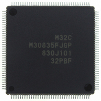
M30835FJGP#U5 Renesas Electronics America, M30835FJGP#U5 Datasheet - Page 97

M30835FJGP#U5
Manufacturer Part Number
M30835FJGP#U5
Description
IC M32C/83 MCU FLASH 144LQFP
Manufacturer
Renesas Electronics America
Series
M16C™ M32C/80r
Datasheets
1.M3087BFLGPU3.pdf
(364 pages)
2.M30833FJGPU3.pdf
(96 pages)
3.M30833FJGPU3.pdf
(529 pages)
Specifications of M30835FJGP#U5
Core Processor
M32C/80
Core Size
16/32-Bit
Speed
32MHz
Connectivity
CAN, I²C, IEBus, SIO, UART/USART
Peripherals
DMA, WDT
Number Of I /o
121
Program Memory Size
512KB (512K x 8)
Program Memory Type
FLASH
Ram Size
31K x 8
Voltage - Supply (vcc/vdd)
3 V ~ 5.5 V
Data Converters
A/D 34x10b, D/A 2x8b
Oscillator Type
Internal
Operating Temperature
-20°C ~ 85°C
Package / Case
144-LQFP
For Use With
R0K330879S001BE - KIT DEV RSK M32C/87R0K330879S000BE - KIT DEV RSK M32C/87
Lead Free Status / RoHS Status
Lead free / RoHS Compliant
Eeprom Size
-
Available stocks
Company
Part Number
Manufacturer
Quantity
Price
Part Number:
M30835FJGP#U5M30835FJGP#U3
Manufacturer:
Renesas Electronics America
Quantity:
10 000
- Current page: 97 of 529
- Download datasheet (5Mb)
R
R
M
e
E
3
. v
J
Figure 8.7 PLC0 and PLV Registers
2
0
1
C
9
3 .
B
8 /
0
1
3
0
3
J
G
4
a
0 -
o r
n
PLL Control Register 0
VDC Control Register for PLL
b7
b7
3 .
1
NOTES:
u
NOTES:
3
, 1
p
b6
0 0 1
b6
1
1. Rewrite the PLC0 register after the PRC0 bit in the PRCR register is set to "1" (write enable).
2. Set these bits when the PLC07 bit is set to "0". Once these bits are set, they cannot be changed.
3. To use the PLL function, the PD8_7 bit in the PD8 register is set to "0" (input) and the CM04 bit in the
4. Before the microcomputer enters wait or stop mode, set the CM17 bit to "0" (main clock as CPU clock
1. Rewrite the PLV register after the PRC3 bit in the PRCR register is set to "1" (write enable).
2. Before the microcomputer enters wait or stop mode, set the CM17 bit to "0" (main clock as CPU
(
2
M
CM0 register is set to "0" (I/O port). Set the PD8_6 bit in the PD8 register to "0" (input) before
connecting P8
source), the PLC07 bit to "0" and PLV00 bit to "0" (cut off power to PLL) in this order.
0
b5
b5
clock source), the PLC07 bit to "0" (PLL off) and PLV00 bit to "0" (cut off power to PLL) in this order.
0
3
6
2
b4
b4
C
8 /
b3
b3
Page 72
, 3
b2
b2
M
6
b1
b1
0
3
to Vss.
2
C
b0
b0
f o
8 /
4
(b7 - b2)
3
8
PLC00
PLC01
PLC02
PLC07
PLV00
Symbol
Symbol
) T
(b3)
(b4)
(b5)
(b6)
8
(b1)
Bit
Bit
Symbol
PLC0
Symbol
PLV
(1)
Programmable Counter
Select Bit
Reserved Bit
Reserved Bit
Reserved Bit
Operation Enable Bit
PLL VDC Enable Bit
Nothing is assigned. When write, set to "0".
When read, its content is indeterminate.
Reserved Bit
Nothing is assigned. When write, set to "0".
When read, its content is indeterminate.
(1)
Bit Name
Bit Name
(2)
Address
0376
Address
0017
(2)
(2)
16
16
(2)
(3, 4)
See Table 8.2
Set to "1"
Set to "0"
Set to "0"
0: PLL is Off
1: PLL is On
Set to "0"
0 : Cut off power to PLL
1 : Power to PLL
After Reset
0011 X100
After Reset
XXXX XX01
Function
Function
2
2
8. Clock Generation Circuit
RW
RW
RW
RW
RW
RW
RW
RW
RW
RW
RW
Related parts for M30835FJGP#U5
Image
Part Number
Description
Manufacturer
Datasheet
Request
R

Part Number:
Description:
KIT STARTER FOR M16C/29
Manufacturer:
Renesas Electronics America
Datasheet:

Part Number:
Description:
KIT STARTER FOR R8C/2D
Manufacturer:
Renesas Electronics America
Datasheet:

Part Number:
Description:
R0K33062P STARTER KIT
Manufacturer:
Renesas Electronics America
Datasheet:

Part Number:
Description:
KIT STARTER FOR R8C/23 E8A
Manufacturer:
Renesas Electronics America
Datasheet:

Part Number:
Description:
KIT STARTER FOR R8C/25
Manufacturer:
Renesas Electronics America
Datasheet:

Part Number:
Description:
KIT STARTER H8S2456 SHARPE DSPLY
Manufacturer:
Renesas Electronics America
Datasheet:

Part Number:
Description:
KIT STARTER FOR R8C38C
Manufacturer:
Renesas Electronics America
Datasheet:

Part Number:
Description:
KIT STARTER FOR R8C35C
Manufacturer:
Renesas Electronics America
Datasheet:

Part Number:
Description:
KIT STARTER FOR R8CL3AC+LCD APPS
Manufacturer:
Renesas Electronics America
Datasheet:

Part Number:
Description:
KIT STARTER FOR RX610
Manufacturer:
Renesas Electronics America
Datasheet:

Part Number:
Description:
KIT STARTER FOR R32C/118
Manufacturer:
Renesas Electronics America
Datasheet:

Part Number:
Description:
KIT DEV RSK-R8C/26-29
Manufacturer:
Renesas Electronics America
Datasheet:

Part Number:
Description:
KIT STARTER FOR SH7124
Manufacturer:
Renesas Electronics America
Datasheet:

Part Number:
Description:
KIT STARTER FOR H8SX/1622
Manufacturer:
Renesas Electronics America
Datasheet:

Part Number:
Description:
KIT DEV FOR SH7203
Manufacturer:
Renesas Electronics America
Datasheet:


