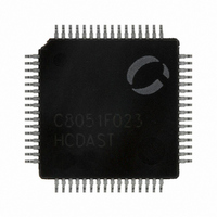
C8051F023R Silicon Laboratories Inc, C8051F023R Datasheet - Page 114

C8051F023R
Manufacturer Part Number
C8051F023R
Description
IC 8051 MCU 64K FLASH 64TQFP
Manufacturer
Silicon Laboratories Inc
Series
C8051F02xr
Specifications of C8051F023R
Core Processor
8051
Core Size
8-Bit
Speed
25MHz
Connectivity
EBI/EMI, SMBus (2-Wire/I²C), SPI, UART/USART
Peripherals
Brown-out Detect/Reset, POR, PWM, Temp Sensor, WDT
Number Of I /o
32
Program Memory Size
64KB (64K x 8)
Program Memory Type
FLASH
Ram Size
4.25K x 8
Voltage - Supply (vcc/vdd)
2.7 V ~ 3.6 V
Data Converters
A/D 8x8b, 8x10b; D/A 2x12b
Oscillator Type
Internal
Operating Temperature
-40°C ~ 85°C
Package / Case
64-TQFP, 64-VQFP
Lead Free Status / RoHS Status
Contains lead / RoHS non-compliant
Eeprom Size
-
Other names
336-1035-2
Available stocks
Company
Part Number
Manufacturer
Quantity
Price
Company:
Part Number:
C8051F023R
Manufacturer:
Silicon Laboratories Inc
Quantity:
10 000
- Current page: 114 of 272
- Download datasheet (2Mb)
C8051F020/1/2/3
114
Bit7:
Bit6:
Bit5:
Bits4-3:
Bit2:
Bit1:
Bit0:
R/W
CY
Bit7
CY: Carry Flag.
This bit is set when the last arithmetic operation resulted in a carry (addition) or a borrow (subtrac-
tion). It is cleared to 0 by all other arithmetic operations.
AC: Auxiliary Carry Flag
This bit is set when the last arithmetic operation resulted in a carry into (addition) or a borrow from
(subtraction) the high order nibble. It is cleared to 0 by all other arithmetic operations.
F0: User Flag 0.
This is a bit-addressable, general purpose flag for use under software control.
RS1-RS0: Register Bank Select.
These bits select which register bank is used during register accesses.
OV: Overflow Flag.
This bit is set to 1 if the last arithmetic operation resulted in a carry (addition), borrow (subtraction),
or overflow (multiply or divide). It is cleared to 0 by all other arithmetic operations.
F1: User Flag 1.
This is a bit-addressable, general purpose flag for use under software control.
PARITY: Parity Flag.
This bit is set to 1 if the sum of the eight bits in the accumulator is odd and cleared if the sum is even.
RS1
0
0
1
1
R/W
AC
Bit6
RS0
0
1
0
1
R/W
Bit5
F0
Figure 12.6. PSW: Program Status Word
Register Bank
RS1
R/W
Bit4
0
1
2
3
Rev. 1.4
RS0
R/W
Bit3
0x08 - 0x0F
0x18 - 0x1F
0x00 - 0x07
0x10 - 0x17
Address
R/W
OV
Bit2
R/W
Bit1
F1
(bit addressable)
PARITY
Bit0
R
SFR Address:
00000000
Reset Value
0xD0
Related parts for C8051F023R
Image
Part Number
Description
Manufacturer
Datasheet
Request
R
Part Number:
Description:
SMD/C°/SINGLE-ENDED OUTPUT SILICON OSCILLATOR
Manufacturer:
Silicon Laboratories Inc
Part Number:
Description:
Manufacturer:
Silicon Laboratories Inc
Datasheet:
Part Number:
Description:
N/A N/A/SI4010 AES KEYFOB DEMO WITH LCD RX
Manufacturer:
Silicon Laboratories Inc
Datasheet:
Part Number:
Description:
N/A N/A/SI4010 SIMPLIFIED KEY FOB DEMO WITH LED RX
Manufacturer:
Silicon Laboratories Inc
Datasheet:
Part Number:
Description:
N/A/-40 TO 85 OC/EZLINK MODULE; F930/4432 HIGH BAND (REV E/B1)
Manufacturer:
Silicon Laboratories Inc
Part Number:
Description:
EZLink Module; F930/4432 Low Band (rev e/B1)
Manufacturer:
Silicon Laboratories Inc
Part Number:
Description:
I°/4460 10 DBM RADIO TEST CARD 434 MHZ
Manufacturer:
Silicon Laboratories Inc
Part Number:
Description:
I°/4461 14 DBM RADIO TEST CARD 868 MHZ
Manufacturer:
Silicon Laboratories Inc
Part Number:
Description:
I°/4463 20 DBM RFSWITCH RADIO TEST CARD 460 MHZ
Manufacturer:
Silicon Laboratories Inc
Part Number:
Description:
I°/4463 20 DBM RADIO TEST CARD 868 MHZ
Manufacturer:
Silicon Laboratories Inc
Part Number:
Description:
I°/4463 27 DBM RADIO TEST CARD 868 MHZ
Manufacturer:
Silicon Laboratories Inc
Part Number:
Description:
I°/4463 SKYWORKS 30 DBM RADIO TEST CARD 915 MHZ
Manufacturer:
Silicon Laboratories Inc
Part Number:
Description:
N/A N/A/-40 TO 85 OC/4463 RFMD 30 DBM RADIO TEST CARD 915 MHZ
Manufacturer:
Silicon Laboratories Inc
Part Number:
Description:
I°/4463 20 DBM RADIO TEST CARD 169 MHZ
Manufacturer:
Silicon Laboratories Inc


