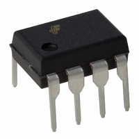
ACE1501EN Fairchild Semiconductor, ACE1501EN Datasheet - Page 19

ACE1501EN
Manufacturer Part Number
ACE1501EN
Description
IC MCU 1KBIT EEPROM 8DIP
Manufacturer
Fairchild Semiconductor
Series
ACEX® 15xxr
Datasheet
1.ACE1501EN.pdf
(33 pages)
Specifications of ACE1501EN
Core Processor
ACE1502
Core Size
8-Bit
Speed
25MHz
Peripherals
Brown-out Detect/Reset, LVD, POR, PWM, WDT
Number Of I /o
6
Program Memory Size
1KB (1K x 8)
Program Memory Type
EEPROM
Eeprom Size
64 x 8
Ram Size
64 x 8
Voltage - Supply (vcc/vdd)
1.8 V ~ 3.6 V
Oscillator Type
Internal
Operating Temperature
-40°C ~ 85°C
Package / Case
8-DIP (0.300", 7.62mm)
Lead Free Status / RoHS Status
Lead free / RoHS Compliant
Data Converters
-
Connectivity
-
ACE1501 Product Family Rev. 1.1
The OCFLAG signal is read only and goes high when the last
encoded bit of the DAT0 frame is transmitting. The OCFLAG sig-
nal is used to inform software that the DAT0 frame transmission
operation is completing (see Figure 25). If multiple DAT0 frames
are to be transmitted consecutively, software should poll the
OCFLAG signal for a 1. Once OCFLAG is 1, DAT0 must be
reload and the START / STOP bit must be restored to 1 in order
to begin the new frame transmission without interruptions (the
synchronization period). Since OCFLAG remains high during
the entire last encoded DAT0 frame bit transmission, software
should wait for the HBC to clear the OCFLAG signal before poll-
ing for the new OCFLAG high pulse. If new data is not reloaded
into DAT0 and the START signal (STOP is active) is not set
before the OCFLAG is 0, the transmission process will end
(TXBUSY is cleared) and a new process will begin starting with
the synchronization period.
Figure 24 and Figure 25 shows how the HBC performs its data
encoding. In the example, two frames are encoded and trans-
mitted consecutively with the following bit encoding format spec-
ification:
1. Transmission frequency = 62.5KHz
2. Data to be encoded = 0x52, 0x92 (all 8-bits)
3. Each bit should be encoded as a 3-bit binary value,
4. Transmission output port : G2
To perform the data transmission, software must first initialize
the PSCALE, BPSEL, HPATTERN, LPATTERN, and DAT0
registers with the appropriate values.
Figure 21. Hardware Bit-coder (HBC) Block Diagram
‘1’ = 110b and ‘0’ = 100b
CLOCK
CPU
Clock Divider
Fixed
by 4
PSCALE
8
[PSCALE]
CLOCK
IR/RF
BPH[2:0]
[BPSEL]
RFCLK
StopShift
RFCLK
StopShift
3
Counter
3
A
Down
Y
3
19
BPL[2:0]
[BPSEL]
B
HPATTERN
LPATTERN
Once the basic registers are initialized, the HBC can be started.
(At the same time, software must set the number of data bits per
data frame and select the desired output port.)
After the HBC has started, software must then poll the OCFLAG
for a high pulse and restore the DAT0 register and the START
signal to continue with the next data transmission.
LOOP_HI:
NXT_FRAME:
If software is to proceed with another data transmission, the
OCFLAG must be zero before polling for the next OCFLAG high
pulse. However, since the specification in the example requires
no other data transmission software can proceed as desired.
LOOP_LO:
LD
LD
LD
LD
LD
LD
IFBIT OCFLAG, HBCNTRL
JP
JP
LD
SBIT
IFBIT OCFLAG, HBCNTRL
JP
Etc.
FRAME[2:0]
[HBCNTRL]
3
NoShift
PSCALE, #03H
BPSEL, #012H
HPATTERN, #0C0H
LPATTERN, #090H
DAT0, #052H
HBCNTRL, #27H
NXT_FRAME
LOOP_HI
DAT0, #092H
START, HBCNTRL
LOOP_LO
ShiftCLK
DAT0
HBCNTRL[7]
OCFLAG
OCFLAG
b7
b7
b7
START/STOP
HBCNTRL[5]
A
B
; (1MHz ?? 4) ?? 4 = 62.5KHz
; BPH = 2, BPL = 2 (3 bits each)
; HPATTERN = 0xC0
; LPATTERN = 0x90
; DAT0 = 0x52
; START / STOP = 1,
FRAME = 7, IOSEL = 0
Y
LOGIC
Sync
HBCNTRL[4]
HBCNTRL[6]
TXBUSY
; Wait for OCFLAG = 1
; DAT0 = 0x92
; START / STOP = 1
; Wait for OCFLAG = 0
; Program proceeds
as desired
IOSEL
www.fairchildsemi.com
G2
G5


