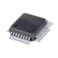
C8051F350 Silicon Laboratories Inc, C8051F350 Datasheet - Page 133

C8051F350
Manufacturer Part Number
C8051F350
Description
IC 8051 MCU 8K FLASH 32LQFP
Manufacturer
Silicon Laboratories Inc
Series
C8051F35xr
Specifications of C8051F350
Core Processor
8051
Core Size
8-Bit
Speed
50MHz
Connectivity
SMBus (2-Wire/I²C), SPI, UART/USART
Peripherals
POR, PWM, Temp Sensor, WDT
Number Of I /o
17
Program Memory Size
8KB (8K x 8)
Program Memory Type
FLASH
Ram Size
768 x 8
Voltage - Supply (vcc/vdd)
2.7 V ~ 3.6 V
Data Converters
A/D 8x24b; D/A 2x8b
Oscillator Type
Internal
Operating Temperature
-40°C ~ 85°C
Package / Case
32-LQFP
Data Bus Width
8 bit
Data Rom Size
128 B
On-chip Adc
10 bit
Number Of Timers
16 bit
Operating Supply Voltage
2.7 V to 3.6 V
Mounting Style
SMD/SMT
Height
1.4 mm
Length
7 mm
Maximum Operating Temperature
+ 85 C
Minimum Operating Temperature
- 40 C
Width
7 mm
Lead Free Status / RoHS Status
Contains lead / RoHS non-compliant
Eeprom Size
-
Lead Free Status / Rohs Status
No RoHS Version Available
Available stocks
Company
Part Number
Manufacturer
Quantity
Price
Company:
Part Number:
C8051F350
Manufacturer:
Silicon Laboratories Inc
Quantity:
10 000
Part Number:
C8051F350
Manufacturer:
SILICON LABS/芯科
Quantity:
20 000
Company:
Part Number:
C8051F350-GQ
Manufacturer:
SiliconL
Quantity:
3 029
Company:
Part Number:
C8051F350-GQ
Manufacturer:
SILICON
Quantity:
18
Company:
Part Number:
C8051F350-GQ
Manufacturer:
Silicon Laboratories Inc
Quantity:
10 000
Company:
Part Number:
C8051F350-GQR
Manufacturer:
Silicon Laboratories Inc
Quantity:
10 000
Part Number:
C8051F350-GQR
Manufacturer:
SILICON LABS/芯科
Quantity:
20 000
Company:
Part Number:
C8051F350DK
Manufacturer:
SiliconL
Quantity:
8
Company:
Part Number:
C8051F350R
Manufacturer:
Silicon Laboratories Inc
Quantity:
10 000
18.
Digital and analog resources are available through 17 I/O pins. Port pins are organized as two byte-wide
Ports and one 1-bit Port. Each of the Port pins can be defined as general-purpose I/O (GPIO) or analog
input/output; Port pins P0.0 - P1.7 can be assigned to one of the internal digital resources as shown in
Figure 18.3. The designer has complete control over which functions are assigned, limited only by the
number of physical I/O pins. This resource assignment flexibility is achieved through the use of a Priority
Crossbar Decoder. Note that the state of a Port I/O pin can always be read in the corresponding Port latch,
regardless of the Crossbar settings.
The Crossbar assigns the selected internal digital resources to the I/O pins based on the Priority Decoder
(Figure 18.3 and Figure 18.4). The registers XBR0 and XBR1, defined in Figure 18.5 and Figure 18.6, are
used to select internal digital functions.
All Port I/Os are 5 V tolerant (refer to Figure 18.2 for the Port cell circuit). The Port I/O cells are configured
as either push-pull or open-drain in the Port Output Mode registers (PnMDOUT, where n = 0,1,2). Com-
plete Electrical Specifications for Port I/O are given in Table 18.1 on page 146.
Highest
Lowest
Priority
Priority
Port Input/Output
SYSCLK
Outputs
SMBus
T0, T1
UART
P0
P1
P2
PCA
CP0
SPI
(P0.0-P0.7)
(P1.0-P1.7)
Figure 18.1. Port I/O Functional Block Diagram
2
2
4
2
4
2
8
8
(P2.0)
Rev. 0.4
PnSKIP Registers
XBR0, XBR1,
Crossbar
Decoder
Priority
Digital
8
8
PnMDIN Registers
PnMDOUT,
C8051F350/1/2/3
Cells
Cells
Cell
I/O
I/O
I/O
P0
P1
P2
P0.0
P0.7
P1.0
P1.7
P2.0
133


