C8051F350 Silicon Laboratories Inc, C8051F350 Datasheet - Page 29
C8051F350
Manufacturer Part Number
C8051F350
Description
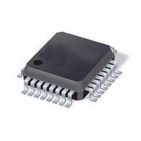
IC 8051 MCU 8K FLASH 32LQFP
Manufacturer
Silicon Laboratories Inc
Series
C8051F35xr
Specifications of C8051F350
Core Processor
8051
Core Size
8-Bit
Speed
50MHz
Connectivity
SMBus (2-Wire/I²C), SPI, UART/USART
Peripherals
POR, PWM, Temp Sensor, WDT
Number Of I /o
17
Program Memory Size
8KB (8K x 8)
Program Memory Type
FLASH
Ram Size
768 x 8
Voltage - Supply (vcc/vdd)
2.7 V ~ 3.6 V
Data Converters
A/D 8x24b; D/A 2x8b
Oscillator Type
Internal
Operating Temperature
-40°C ~ 85°C
Package / Case
32-LQFP
Data Bus Width
8 bit
Data Rom Size
128 B
On-chip Adc
10 bit
Number Of Timers
16 bit
Operating Supply Voltage
2.7 V to 3.6 V
Mounting Style
SMD/SMT
Height
1.4 mm
Length
7 mm
Maximum Operating Temperature
+ 85 C
Minimum Operating Temperature
- 40 C
Width
7 mm
Lead Free Status / RoHS Status
Contains lead / RoHS non-compliant
Eeprom Size
-
Lead Free Status / Rohs Status
No RoHS Version Available
Available stocks
Company
Part Number
Manufacturer
Quantity
Price
Company:

Part Number:
C8051F350
Manufacturer:
Silicon Laboratories Inc
Quantity:
10 000
Part Number:
C8051F350
Manufacturer:
SILICON LABS/芯科
Quantity:
20 000
Company:
Part Number:
C8051F350-GQ
Manufacturer:
SiliconL
Quantity:
3 029
Company:
Part Number:
C8051F350-GQ
Manufacturer:
SILICON
Quantity:
18
Company:
Part Number:
C8051F350-GQ
Manufacturer:
Silicon Laboratories Inc
Quantity:
10 000
Company:
Part Number:
C8051F350-GQR
Manufacturer:
Silicon Laboratories Inc
Quantity:
10 000
Part Number:
C8051F350-GQR
Manufacturer:
SILICON LABS/芯科
Quantity:
20 000
Company:
Part Number:
C8051F350DK
Manufacturer:
SiliconL
Quantity:
8
Company:
Part Number:
C8051F350R
Manufacturer:
Silicon Laboratories Inc
Quantity:
10 000


4.
XTAL1
XTAL2
DGND
AGND
Name
C2CK
P2.0/
P0.2/
P0.3/
/RST
C2D
P0.0
P0.1
P0.4
P0.5
AV+
V
Pinout and Package Definitions
DD
Pin Numbers
‘F350
‘F352
21
22
10
12
13
14
15
16
17
18
11
Table 4.1. Pin Definitions for the C8051F350/1/2/3
9
‘F351
‘F353
17
18
10
12
13
14
11
6
5
8
7
9
D I/O or
D I/O or
D I/O or
D I/O or
D I/O or
A I/O or
Ground Digital Ground. Must be tied to Ground.
Ground Analog Ground. Must be tied to Ground.
Power
Power
Type
D I/O
D I/O
D I/O
D I/O
D I/O
A In
A In
A In
A In
D In
A In
A In
Description
Digital Supply Voltage. Must be tied to +2.7 V to +3.6 V
power.
Analog Supply Voltage. Must be tied to +2.7 V to +3.6 V
power.
Device Reset. Open-drain output of internal POR or V
monitor. An external source can initiate a system reset by
driving this pin low for at least 15 µs. A 1kΩ pull-up to V
recommended. See Reset Sources Section.
Clock signal for the C2 Debug Interface.
Port 2.0. See Port I/O Section for a complete description.
Bi-directional data signal for the C2 Debug Interface.
Port 0.0. See Port I/O Section for a complete description.
Port 0.1. See Port I/O Section for a complete description.
Port 0.2. See Port I/O Section for a complete description.
This pin is the external oscillator return for a crystal or reso-
nator. See Oscillator Section.
Port 0.3. See Port I/O Section for a complete description.
This pin is the excitation driver for an external crystal or res-
onator, or an external clock input for CMOS, capacitor, or
RC oscillator configurations. See Oscillator Section.
Port 0.4. See Port I/O Section for a complete description.
Port 0.5. See Port I/O Section for a complete description.
Rev. 0.4
C8051F350/1/2/3
DD
DD
is
29
Related parts for C8051F350
Image
Part Number
Description
Manufacturer
Datasheet
Request
R

Part Number:
Description:
SMD/C°/SINGLE-ENDED OUTPUT SILICON OSCILLATOR
Manufacturer:
Silicon Laboratories Inc
Part Number:
Description:
Manufacturer:
Silicon Laboratories Inc
Datasheet:
Part Number:
Description:
N/A N/A/SI4010 AES KEYFOB DEMO WITH LCD RX
Manufacturer:
Silicon Laboratories Inc
Datasheet:
Part Number:
Description:
N/A N/A/SI4010 SIMPLIFIED KEY FOB DEMO WITH LED RX
Manufacturer:
Silicon Laboratories Inc
Datasheet:
Part Number:
Description:
N/A/-40 TO 85 OC/EZLINK MODULE; F930/4432 HIGH BAND (REV E/B1)
Manufacturer:
Silicon Laboratories Inc
Part Number:
Description:
EZLink Module; F930/4432 Low Band (rev e/B1)
Manufacturer:
Silicon Laboratories Inc
Part Number:
Description:
I°/4460 10 DBM RADIO TEST CARD 434 MHZ
Manufacturer:
Silicon Laboratories Inc
Part Number:
Description:
I°/4461 14 DBM RADIO TEST CARD 868 MHZ
Manufacturer:
Silicon Laboratories Inc
Part Number:
Description:
I°/4463 20 DBM RFSWITCH RADIO TEST CARD 460 MHZ
Manufacturer:
Silicon Laboratories Inc
Part Number:
Description:
I°/4463 20 DBM RADIO TEST CARD 868 MHZ
Manufacturer:
Silicon Laboratories Inc
Part Number:
Description:
I°/4463 27 DBM RADIO TEST CARD 868 MHZ
Manufacturer:
Silicon Laboratories Inc
Part Number:
Description:
I°/4463 SKYWORKS 30 DBM RADIO TEST CARD 915 MHZ
Manufacturer:
Silicon Laboratories Inc
Part Number:
Description:
N/A N/A/-40 TO 85 OC/4463 RFMD 30 DBM RADIO TEST CARD 915 MHZ
Manufacturer:
Silicon Laboratories Inc
Part Number:
Description:
I°/4463 20 DBM RADIO TEST CARD 169 MHZ
Manufacturer:
Silicon Laboratories Inc