C8051F350 Silicon Laboratories Inc, C8051F350 Datasheet - Page 48
C8051F350
Manufacturer Part Number
C8051F350
Description
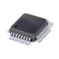
IC 8051 MCU 8K FLASH 32LQFP
Manufacturer
Silicon Laboratories Inc
Series
C8051F35xr
Specifications of C8051F350
Core Processor
8051
Core Size
8-Bit
Speed
50MHz
Connectivity
SMBus (2-Wire/I²C), SPI, UART/USART
Peripherals
POR, PWM, Temp Sensor, WDT
Number Of I /o
17
Program Memory Size
8KB (8K x 8)
Program Memory Type
FLASH
Ram Size
768 x 8
Voltage - Supply (vcc/vdd)
2.7 V ~ 3.6 V
Data Converters
A/D 8x24b; D/A 2x8b
Oscillator Type
Internal
Operating Temperature
-40°C ~ 85°C
Package / Case
32-LQFP
Data Bus Width
8 bit
Data Rom Size
128 B
On-chip Adc
10 bit
Number Of Timers
16 bit
Operating Supply Voltage
2.7 V to 3.6 V
Mounting Style
SMD/SMT
Height
1.4 mm
Length
7 mm
Maximum Operating Temperature
+ 85 C
Minimum Operating Temperature
- 40 C
Width
7 mm
Lead Free Status / RoHS Status
Contains lead / RoHS non-compliant
Eeprom Size
-
Lead Free Status / Rohs Status
No RoHS Version Available
Available stocks
Company
Part Number
Manufacturer
Quantity
Price
Company:

Part Number:
C8051F350
Manufacturer:
Silicon Laboratories Inc
Quantity:
10 000
Part Number:
C8051F350
Manufacturer:
SILICON LABS/芯科
Quantity:
20 000
Company:
Part Number:
C8051F350-GQ
Manufacturer:
SiliconL
Quantity:
3 029
Company:
Part Number:
C8051F350-GQ
Manufacturer:
SILICON
Quantity:
18
Company:
Part Number:
C8051F350-GQ
Manufacturer:
Silicon Laboratories Inc
Quantity:
10 000
Company:
Part Number:
C8051F350-GQR
Manufacturer:
Silicon Laboratories Inc
Quantity:
10 000
Part Number:
C8051F350-GQR
Manufacturer:
SILICON LABS/芯科
Quantity:
20 000
Company:
Part Number:
C8051F350DK
Manufacturer:
SiliconL
Quantity:
8
Company:
Part Number:
C8051F350R
Manufacturer:
Silicon Laboratories Inc
Quantity:
10 000


C8051F350/1/2/3
48
Bit 7:
Bit 6:
Bits 5-4: RESERVED: Must Write to 00b.
Bit 3:
Bits 2-0: AD0SM: ADC0 System Mode Select.
AD0EN
R/W
Bit7
AD0EN: ADC0 Enable Bit.
0: ADC0 Disabled. ADC is in low-power shutdown.
1: ADC0 Enabled. ADC is active and ready to perform calibrations or conversions.
Note: Disabling the ADC automatically resets the AD0SM bits back to the "Idle" state.
Unused: Read = 0b, Write = don’t care.
Unused: Read = 0b, Write = don’t care.
These bits define the operating mode for the ADC. They are used to initiate all ADC conver-
sion and calibration cycles.
000: Idle
001: Full Internal Calibration (offset and gain).
010: Single Conversion.
011: Continuous Conversion.
100: Internal Offset Calibration.
101: Internal Gain Calibration.
110: System Offset Calibration.
111: System Gain Calibration.
Note: Any system mode change by the user during a conversion or calibration will
terminate the operation, and corrupt the result. To write to many of the other ADC reg-
isters, the AD0SM bits must be set to IDLE mode (000b).
Bit6
R
-
Reserved Reserved
Figure 5.7. ADC0MD: ADC0 Mode Register
R/W
Bit5
R/W
Bit4
Rev. 0.4
Bit3
R
-
R/W
Bit2
AD0SM
R/W
Bit1
SFR Address:
R/W
Bit0
0xF3
00000000
Reset Value
Related parts for C8051F350
Image
Part Number
Description
Manufacturer
Datasheet
Request
R

Part Number:
Description:
SMD/C°/SINGLE-ENDED OUTPUT SILICON OSCILLATOR
Manufacturer:
Silicon Laboratories Inc
Part Number:
Description:
Manufacturer:
Silicon Laboratories Inc
Datasheet:
Part Number:
Description:
N/A N/A/SI4010 AES KEYFOB DEMO WITH LCD RX
Manufacturer:
Silicon Laboratories Inc
Datasheet:
Part Number:
Description:
N/A N/A/SI4010 SIMPLIFIED KEY FOB DEMO WITH LED RX
Manufacturer:
Silicon Laboratories Inc
Datasheet:
Part Number:
Description:
N/A/-40 TO 85 OC/EZLINK MODULE; F930/4432 HIGH BAND (REV E/B1)
Manufacturer:
Silicon Laboratories Inc
Part Number:
Description:
EZLink Module; F930/4432 Low Band (rev e/B1)
Manufacturer:
Silicon Laboratories Inc
Part Number:
Description:
I°/4460 10 DBM RADIO TEST CARD 434 MHZ
Manufacturer:
Silicon Laboratories Inc
Part Number:
Description:
I°/4461 14 DBM RADIO TEST CARD 868 MHZ
Manufacturer:
Silicon Laboratories Inc
Part Number:
Description:
I°/4463 20 DBM RFSWITCH RADIO TEST CARD 460 MHZ
Manufacturer:
Silicon Laboratories Inc
Part Number:
Description:
I°/4463 20 DBM RADIO TEST CARD 868 MHZ
Manufacturer:
Silicon Laboratories Inc
Part Number:
Description:
I°/4463 27 DBM RADIO TEST CARD 868 MHZ
Manufacturer:
Silicon Laboratories Inc
Part Number:
Description:
I°/4463 SKYWORKS 30 DBM RADIO TEST CARD 915 MHZ
Manufacturer:
Silicon Laboratories Inc
Part Number:
Description:
N/A N/A/-40 TO 85 OC/4463 RFMD 30 DBM RADIO TEST CARD 915 MHZ
Manufacturer:
Silicon Laboratories Inc
Part Number:
Description:
I°/4463 20 DBM RADIO TEST CARD 169 MHZ
Manufacturer:
Silicon Laboratories Inc