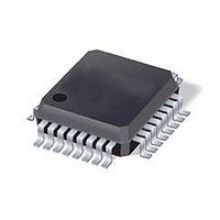
C8051F350 Silicon Laboratories Inc, C8051F350 Datasheet - Page 62

C8051F350
Manufacturer Part Number
C8051F350
Description
IC 8051 MCU 8K FLASH 32LQFP
Manufacturer
Silicon Laboratories Inc
Series
C8051F35xr
Specifications of C8051F350
Core Processor
8051
Core Size
8-Bit
Speed
50MHz
Connectivity
SMBus (2-Wire/I²C), SPI, UART/USART
Peripherals
POR, PWM, Temp Sensor, WDT
Number Of I /o
17
Program Memory Size
8KB (8K x 8)
Program Memory Type
FLASH
Ram Size
768 x 8
Voltage - Supply (vcc/vdd)
2.7 V ~ 3.6 V
Data Converters
A/D 8x24b; D/A 2x8b
Oscillator Type
Internal
Operating Temperature
-40°C ~ 85°C
Package / Case
32-LQFP
Data Bus Width
8 bit
Data Rom Size
128 B
On-chip Adc
10 bit
Number Of Timers
16 bit
Operating Supply Voltage
2.7 V to 3.6 V
Mounting Style
SMD/SMT
Height
1.4 mm
Length
7 mm
Maximum Operating Temperature
+ 85 C
Minimum Operating Temperature
- 40 C
Width
7 mm
Lead Free Status / RoHS Status
Contains lead / RoHS non-compliant
Eeprom Size
-
Lead Free Status / Rohs Status
No RoHS Version Available
Available stocks
Company
Part Number
Manufacturer
Quantity
Price
Company:
Part Number:
C8051F350
Manufacturer:
Silicon Laboratories Inc
Quantity:
10 000
Part Number:
C8051F350
Manufacturer:
SILICON LABS/芯科
Quantity:
20 000
Company:
Part Number:
C8051F350-GQ
Manufacturer:
SiliconL
Quantity:
3 029
Company:
Part Number:
C8051F350-GQ
Manufacturer:
SILICON
Quantity:
18
Company:
Part Number:
C8051F350-GQ
Manufacturer:
Silicon Laboratories Inc
Quantity:
10 000
Company:
Part Number:
C8051F350-GQR
Manufacturer:
Silicon Laboratories Inc
Quantity:
10 000
Part Number:
C8051F350-GQR
Manufacturer:
SILICON LABS/芯科
Quantity:
20 000
Company:
Part Number:
C8051F350DK
Manufacturer:
SiliconL
Quantity:
8
Company:
Part Number:
C8051F350R
Manufacturer:
Silicon Laboratories Inc
Quantity:
10 000
C8051F350/1/2/3
6.1.
A flexible output update mechanism allows for seamless full-scale changes and supports jitter-free
updates for waveform generation. Three update modes are provided, allowing IDAC output updates on a
write to the IDAC’s data register, on a Timer overflow, or on an external pin edge.
6.1.1. Update Output On-Demand
In its default mode (IDAnCN.[6:4] = ‘111’) the IDAC output is updated “on-demand” with a write to the data
register (IDAn). In this mode, data is immediately latched into the IDAC after a write to its data register.
6.1.2. Update Output Based on Timer Overflow
The IDAC output update can be scheduled on a Timer overflow. This feature is useful in systems where the
IDAC is used to generate a waveform of a defined sampling rate, by eliminating the effects of variable
interrupt latency and instruction execution on the timing of the IDAC output. When the IDAnCM bits
(IDAnCN.[6:4]) are set to ‘000’, ‘001’, ‘010’ or ‘011’, writes to the IDAC data register (IDAn) are held until an
associated Timer overflow event (Timer 0, Timer 1, Timer 2 or Timer 3, respectively) occurs, at which time
the data register contents are copied to the IDAC input latch, allowing the IDAC output to change to the
new value.
6.1.3. Update Output Based on CNVSTR Edge
The IDAC output can also be configured to update on a rising edge, falling edge, or both edges of the
external CNVSTR signal. When the IDAnCM bits (IDAnCN.[6:4]) are set to ‘100’, ‘101’, or ‘110’, writes to
the IDAC data register (IDAn) are held until an edge occurs on the CNVSTR input pin. The particular set-
ting of the IDAnCM bits determines whether the IDAC output is updated on rising, falling, or both edges of
CNVSTR. When a corresponding edge occurs, the data register contents are copied to the IDAC input
latch, allowing the IDAC output to change to the new value.
6.2.
The data word mapping for the IDAC is shown in Figure 6.2. The full-scale output current of the IDAC is
selected using the IDAnOMD bits (IDAnCN[1:0]). By default, the IDAC is set to a full-scale output current of
0.25 mA. The IDAnOMD bits can also be configured to provide full-scale output currents of 0.5 mA, 1 mA,
or 2 mA.
62
IDAn Data Word
(D7 - D0)
IDAC Output Scheduling
IDAC Output Mapping
0xFF
0x00
0x01
0x80
128/256 x 2 mA
255/256 x 2 mA
1/256 x 2 mA
‘11’ (2 mA)
Figure 6.2. IDAC Data Word Mapping
0 mA
Output Current vs IDAnOMD bit setting
128/256 x 1 mA
255/256 x 1 mA
1/256 x 1 mA
‘10’ (1 mA)
Rev. 0.4
0 mA
128/256 x 0.5 mA 128/256 x 0.25 mA
255/256 x 0.5 mA 255/256 x 0.25 mA
1/256 x 0.5 mA
‘01’ (0.5 mA)
0 mA
1/256 x 0.25 mA
‘00’ (0.25 mA)
0 mA


