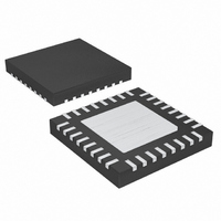
MAX3798ETJ+ Maxim Integrated Products, MAX3798ETJ+ Datasheet - Page 16

MAX3798ETJ+
Manufacturer Part Number
MAX3798ETJ+
Description
IC LIMITING AMP/VCSEL DVR 32TQFN
Manufacturer
Maxim Integrated Products
Datasheet
1.MAX3798ETJ.pdf
(35 pages)
Specifications of MAX3798ETJ+
Amplifier Type
Limiting
Number Of Circuits
1
Output Type
Differential
Current - Supply
97mA
Voltage - Supply, Single/dual (±)
2.85 V ~ 3.63 V
Operating Temperature
-40°C ~ 85°C
Mounting Type
Surface Mount
Package / Case
32-TQFN Exposed Pad
Operating Temperature Range
+ 85 C
Mounting Style
SMD/SMT
Lead Free Status / RoHS Status
Lead free / RoHS Compliant
Current - Output / Channel
-
-3db Bandwidth
-
Slew Rate
-
Gain Bandwidth Product
-
Current - Input Bias
-
Voltage - Input Offset
-
Lead Free Status / Rohs Status
Details
1.0625Gbps to 10.32Gbps, Integrated, Low-
Power SFP+ Limiting Amplifier and VCSEL Driver
The limiting amplifier features a high-gain mode and a
high-bandwidth mode allowing for overall system opti-
mization. Either the MSEL pin or the MODE_SEL bit can
perform the mode selection. For operating up to
4.25Gbps, the high-gain mode (MODE_SEL = 0) is rec-
ommended. For operating above 8.5Gbps, the high-
bandwidth mode (MODE_SEL = 1) is recommended.
For operations at 8.5Gbps, the mode selection is
dependent on the performance of the receiver optical
subassembly. The polarity of ROUT+/ROUT- relative to
RIN+/RIN- is programmed by the RX_POL bit.
The offset correction circuit is enabled to remove pulse-
width distortion caused by intrinsic offset voltages with-
in the differential amplifier stages. An external capacitor
(C
used to set the offset correction loop cutoff frequency.
The offset loop can be disabled using the AZ_EN bit.
The MAX3798 contains a feature that allows the part to
meet a 10μs mode-select switching time. The mode-
select switching time can be adjusted using the GMEN
and CAZX bits.
The CML output stage is optimized for differential 100Ω
loads. The RXDE_EN bit adds analog deemphasis
compensation to the limited differential output signal for
SFP connector losses. The output stage is controlled by
a combination of the RX_EN and SQ_EN bits and the
LOS pin. See Table 1.
Amplitude of the CML output stage is controlled by an
8-bit DAC register (SET_CML). The differential output
amplitude range is from 40mV
Table 1. CML Output Stage Operation Mode
16
RX_EN
AZ
) connected between the CAZ1 and CAZ2 pins is
______________________________________________________________________________________
0
1
1
1
CML Output Stage with Deemphasis and
SQ_EN
X
0
1
1
LOS
X
X
0
1
Offset Correction Circuitry
P-P
CML output disabled.
CML output enabled.
CML output enabled.
CML output disabled.
up to 1200mV
OPERATION MODE
Slew-Rate Control
Dual Path Limiter
DESCRIPTION
P-P
with
4.6mV
tial load).
The lower bandwidth data path allows for reduction of
output edge speed in order to enhance EMI perfor-
mance. The SLEW_RATE bit controls the slew rate of
the output stage (see Table 2).
The input data amplitude is compared to a preset
threshold controlled by the 6-bit DAC register
SET_LOS. The LOS assert level can be programmed
from 14mV
(assuming an ideal 100Ω differential source). LOS is
enabled through the LOS_EN bit and the polarity of the
LOS is controlled with the LOS_POL bit.
The VCSEL driver inside the MAX3798 is designed to
operate from 1.0625Gbps to 10.32Gbps. The transmit-
ter contains a differential data path with pulse-width
adjustment, bias current and modulation current DACs,
output driver with programmable deemphasis, power-
on reset circuitry, BIAS monitor, VCSEL current limiter,
and eye safety circuitry. A 3-wire digital interface is
used to control the transmitter functions. The registers
that control the transmitter functionality are TXCTRL,
TXSTAT1, TXSTAT2, SET_IBIAS, SET_IMOD, IMOD-
MAX, IBIASMAX, MODINC, BIASINC, MODECTRL,
SET_PWCTRL, and SET_TXDE.
The CML input buffer is optimized for AC-coupled sig-
nals and is internally terminated with a differential 100Ω.
Differential input data is equalized for high-frequency
losses due to SFP connectors. The TX_POL bit in the
TXCTRL register controls the polarity of TOUT+ and
TOUT- vs. TIN+ and TIN-. The SET_PWCTRL register
Table 2. Slew-Rate Control for CML
Output Stage
MODE_SEL
0
0
1
P-P
resolution (assuming an ideal 100Ω differen-
P-P
SLEW_RATE
up to 77mV
0
1
X
Loss-of-Signal (LOS) Circuitry
P-P
4.25Gbps operation with
reduced output edge speed.
4.25Gbps operation with full
edge speed; 8.5Gbps
operation with high bandwidth
ROSA.
8.5Gbps with lower bandwidth
ROSA; 10.32Gbps operation.
with 1.5mV
OPERATION MODE
Differential Data Path
DESCRIPTION
VCSEL Driver
P-P
resolution


