MAX3798ETJ+ Maxim Integrated Products, MAX3798ETJ+ Datasheet - Page 5

MAX3798ETJ+
Manufacturer Part Number
MAX3798ETJ+
Description
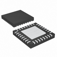
IC LIMITING AMP/VCSEL DVR 32TQFN
Manufacturer
Maxim Integrated Products
Datasheet
1.MAX3798ETJ.pdf
(35 pages)
Specifications of MAX3798ETJ+
Amplifier Type
Limiting
Number Of Circuits
1
Output Type
Differential
Current - Supply
97mA
Voltage - Supply, Single/dual (±)
2.85 V ~ 3.63 V
Operating Temperature
-40°C ~ 85°C
Mounting Type
Surface Mount
Package / Case
32-TQFN Exposed Pad
Operating Temperature Range
+ 85 C
Mounting Style
SMD/SMT
Lead Free Status / RoHS Status
Lead free / RoHS Compliant
Current - Output / Channel
-
-3db Bandwidth
-
Slew Rate
-
Gain Bandwidth Product
-
Current - Input Bias
-
Voltage - Input Offset
-
Lead Free Status / Rohs Status
Details
ELECTRICAL CHARACTERISTICS (continued)
(V
put load is AC-coupled to differential 100Ω (see Figure 1), typical values are at +25°C, V
otherwise specified. Registers are set to default values unless otherwise noted, and the 3-wire interface is static during measure-
ments. For testing, the MODE_SEL bit was used and the MSEL pin was left open.)
Power SFP+ Limiting Amplifier and VCSEL Driver
Random Jitter
Output Return Loss
Tx BIAS GENERATOR
Maximum Bias-On Current
Minimum Bias-On Current
BIAS Current DAC Stability
Compliance Voltage at BIAS
BIAS Current Monitor Current
Gain
Compliance Voltage at BMON
BIAS Current Monitor Current
Gain Stability
Tx SAFETY FEATURES
Excessive Voltage at BMAX
Excessive Voltage at MMAX
Excessive Voltage at BMON
Excessive Voltage at BIAS
Maximum VCSEL Current in Off
State
SFP TIMING REQUIREMENTS
Mode-Select Change Time
DISABLE Assert Time
CC
= 2.85V to 3.63V, T
PARAMETER
1.0625Gbps to 10.32Gbps, Integrated, Low-
_______________________________________________________________________________________
A
= -40°C to +85°C, CML receiver output load is AC-coupled to differential 100Ω, C
t_
SYMBOL
I
I
BIASMAX
BIASMIN
MODESEL
SDD22
V
V
V
V
I
I
V
V
t_
BMON
BMON
BMON
BMON
MMAX
I
BMAX
BIAS
BIAS
OFF
OFF
5mA
800mV
DUT is powered on, f
DUT is powered on, f
Current into BIAS pin
Current into BIAS pin
2mA
External resistor to GND defines the
voltage gain
2mA
Average voltage, FAULT always occurs for
V
for V
Average voltage, FAULT always occurs for
V
for V
Average voltage, FAULT warning always
occurs for V
warning never occurs for V
0.65V
Average voltage, FAULT always occurs for
V
V
FAULT or DISABLE, V
Time from rising or falling edge at MSEL
until Rx output PWD falls below 10ps
Time from rising edge of DISABLE input
signal to I
I
MODOFF
BMAX
MMAX
BIAS
BIAS
BMAX
MMAX
P-P
I
I
I
MOD
BIAS
BIAS
0.44V, FAULT never occurs for
0.65V
V
V
BIAS
CC
CC
BMON
V
V
- 0.65V, FAULT never occurs
CC
CC
- 0.65V, FAULT never occurs
12mA, 250mV
15mA (Notes 2, 10)
15mA (Note 10)
CONDITIONS
= I
- 0.55V
- 0.55V
BIASOFF
V
CC
BIAS
5GHz
16GHz
- 0.55V, FAULT
and I
BMON
= V
P-P
CC
MOD
V
V
IN
CC
=
CC
-
= 3.3V, I
0.65V
0.65V
0.65V
V
V
V
0.44
MIN
0.9
CC
CC
CC
15
0
BIAS
-
-
-
= 6mA, I
V
V
V
TYP
0.17
0.6V
0.6V
0.6V
0.48
12
16
CC
CC
CC
10
AZ
5
-
-
-
= 1nF, transmitter out-
MOD
0.55V
0.55V
0.55V
V
V
V
MAX
0.65
0.5
2.1
1.8
CC
CC
CC
25
2
4
5
1
= 6mA, unless
-
-
-
UNITS
ps
mA/A
mA
mA
dB
μA
μs
μs
%
%
RMS
V
V
V
V
V
V
5


